Stack packaging structure
A technology of packaging structure and chip packaging structure, which is applied in the direction of semiconductor/solid-state device parts, semiconductor devices, electrical components, etc., can solve the problems that affect the reliability of stacked packaging structure, reduce the yield of packaging process, and incomplete bonding, etc. Achieve the effects of preventing false soldering, improving yield and reducing area
- Summary
- Abstract
- Description
- Claims
- Application Information
AI Technical Summary
Problems solved by technology
Method used
Image

Examples
Embodiment Construction
[0019] Relevant detailed description and technical contents of the present invention are as follows now in conjunction with the accompanying drawings:
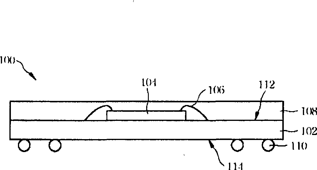
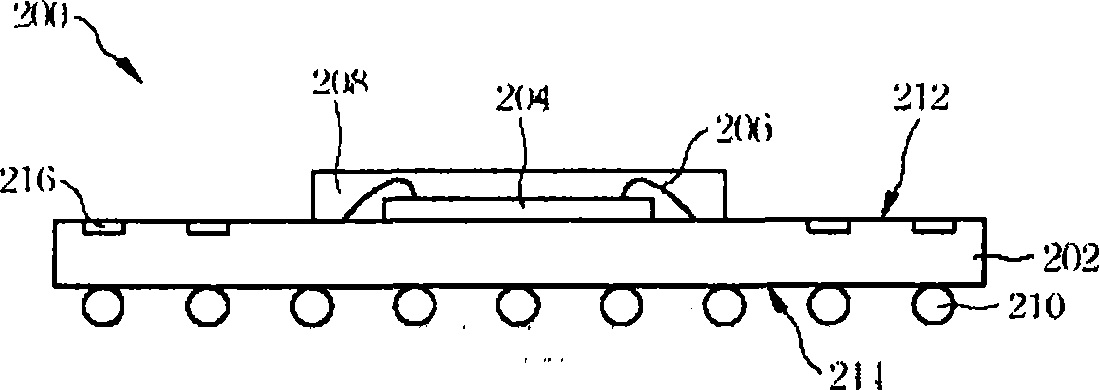
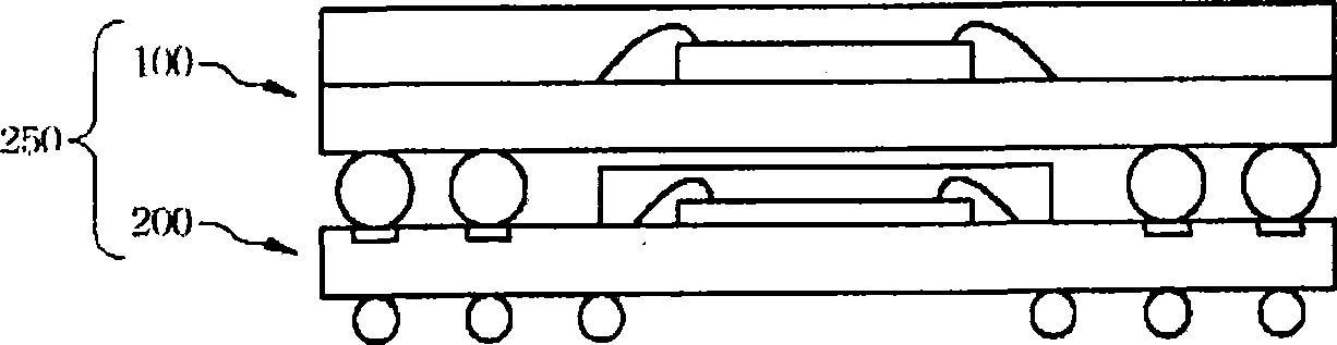
[0020] Figure 4 to Figure 9B It is a process sectional view of a stacked packaging structure according to a preferred embodiment of the present invention, and please also refer to Figure 12A . When making the stacked package structure of the present invention, first make the chip package structure 324a, for example Figure 8 structure shown. When fabricating the chip package structure 324a, the substrate 300a or the substrate 300b is provided first, wherein the substrate 300a or the substrate 300b may be a printed circuit board (PCB). The substrate 300a has an opposite surface 326a and a surface 328a, and the substrate 300b has an opposite surface 326b and a surface 328b. It should be noted that when the substrate 300b is provided by the supplier, several electrical connection elements 312d have been provided on the surf...
PUM
 Abstract
Description
Claims
Application Information
 - R&D Engineer
- R&D Manager
- IP Professional
- Industry Leading Data Capabilities
- Powerful AI technology
- Patent DNA Extraction
Browse by: Latest US Patents, China's latest patents, Technical Efficacy Thesaurus, Application Domain, Technology Topic.
© 2024 PatSnap. All rights reserved.Legal|Privacy policy|Modern Slavery Act Transparency Statement|Sitemap