Supercharge Your Innovation With Domain-Expert AI Agents!

Memory cell test circuit for semiconductor memory device and its method

A storage unit and test circuit technology, which is applied in information storage, static memory, digital memory information, etc., can solve the problems of increasing the size of traditional SDRSDRAM and increasing the size of test circuits

Inactive Publication Date: 2009-09-23
SK HYNIX INC
View PDF4 Cites 0 Cited by
  • Summary
  • Abstract
  • Description
  • Claims
  • Application Information

AI Technical Summary

Problems solved by technology

[0034] However, as mentioned above, each bank of conventional SDR SDRAM includes test global input / output lines and a logic operation unit, which increases the size of conventional SDR SDRAM
Moreover, if the above-mentioned test circuit is used for a double data rate (DDR) SDRAM or DD2 SDRAM, the size of the test circuit will be further increased

Method used


Image

  • Memory cell test circuit for semiconductor memory device and its method
  • Memory cell test circuit for semiconductor memory device and its method
  • Memory cell test circuit for semiconductor memory device and its method

Examples


Embodiment Construction

[0046] Hereinafter, a memory cell testing circuit according to the present invention will be described in detail with reference to the accompanying drawings.

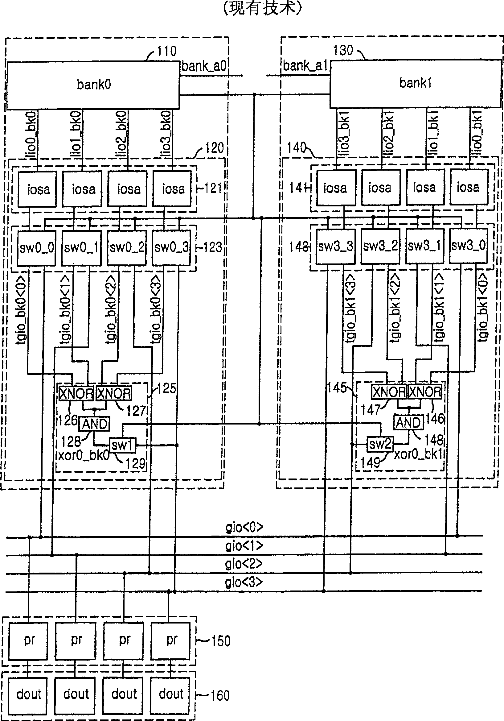
[0047] Figure 4 It is a block diagram showing a semiconductor memory device including a memory cell test circuit according to a preferred embodiment of the present invention.

[0048] As shown in the figure, the semiconductor storage device includes a first memory bank unit 410 , a second memory bank unit 420 , a multi-clock generator 440 , a logic operation unit 450 , a switch unit 460 , a pipeline unit 470 and a data output unit 480 .

[0049] The first memory bank unit 410 includes a first memory bank 411 with a plurality of memory cells for outputting data to the first memory bank first to first memory bank fourth local input / output lines lio0_bk0 to lio3_bk0; the first input / output sense amplifier (IOSA) unit 413 for amplifying the signal level of data output to the first bank first to first bank fourth local in...


PUM


Abstract

A memory cell test circuit used in a semiconductor memory device having a plurality of memory banks connected to a plurality of global input / output lines, comprising: a plurality of memory bank switching units for controlling based on a test mode signal and a plurality of A clock signal transmits data output from a plurality of memory banks to a plurality of global input / output lines; a logical operation unit is used to perform a logical operation on data output to a plurality of global input / output lines and to output a result of the logical operation to a test global input / output line; and a switch unit coupled to the test global input / output line and the plurality of global input / output lines for selectively passing the test global input based on the test mode signal and the plurality of control clock signals / Output line data and global I / O line data.

Description

technical field [0001] The present invention relates to a semiconductor memory device, and more particularly, to a circuit for testing memory cells included in the semiconductor memory device. Background technique [0002] Since a semiconductor memory device is highly integrated, the test time taken for testing a memory cell included in the semiconductor memory device is increased. Therefore, recently, a test circuit capable of testing a plurality of memory cells at a time has been developed. That is, the test circuit tests the plurality of memory cells by inputting the same logic data to the plurality of memory cells and detecting output logic values ​​generated by performing a logic operation to output values ​​of the plurality of memory cells. [0003] figure 1 A block diagram for testing a memory cell showing a conventional single data rate synchronous semiconductor memory (SDR SDRAM) device. It is assumed here that the traditional SDR SDRAM includes two banks. [00...

Claims


Application Information

Patent Timeline
Patent Type & Authority Patents(China)
IPC IPC(8): G11C7/24G11C29/00
CPCG11C29/1201G11C29/48G11C29/26G11C11/4076G11C11/4091
Inventor 李昶赫
Owner SK HYNIX INC
Features
  • R&D
  • Intellectual Property
  • Life Sciences
  • Materials
  • Tech Scout
  • Unparalleled Data Quality
  • Higher Quality Content
  • 60% Fewer Hallucinations
Learn More