Transverse electric-injection luminescent device of indirect gap semiconductor material controlled by phonon

A technology of light-emitting devices and semiconductors, applied in semiconductor devices, electrical components, circuits, etc., can solve the problems of incompatibility and difficulty in large-scale integrated circuit processes, and achieve process compatibility, easy implementation, and enhanced luminous efficiency and intensity Effect

Inactive Publication Date: 2009-10-21
INST OF SEMICONDUCTORS - CHINESE ACAD OF SCI
View PDF3 Cites 0 Cited by
  • Summary
  • Abstract
  • Description
  • Claims
  • Application Information

AI Technical Summary

Problems solved by technology

The general international effort is to reduce the dimension of silicon-based materials in order to achieve quantum confinement effect or direct bandgap silicon-based materials to achieve efficient silicon-based light emission, but it is very difficult and not too compatible with large-scale integrated circuit technology. compatible

Method used


Image

  • Transverse electric-injection luminescent device of indirect gap semiconductor material controlled by phonon
  • Transverse electric-injection luminescent device of indirect gap semiconductor material controlled by phonon

Examples


no. 1 example

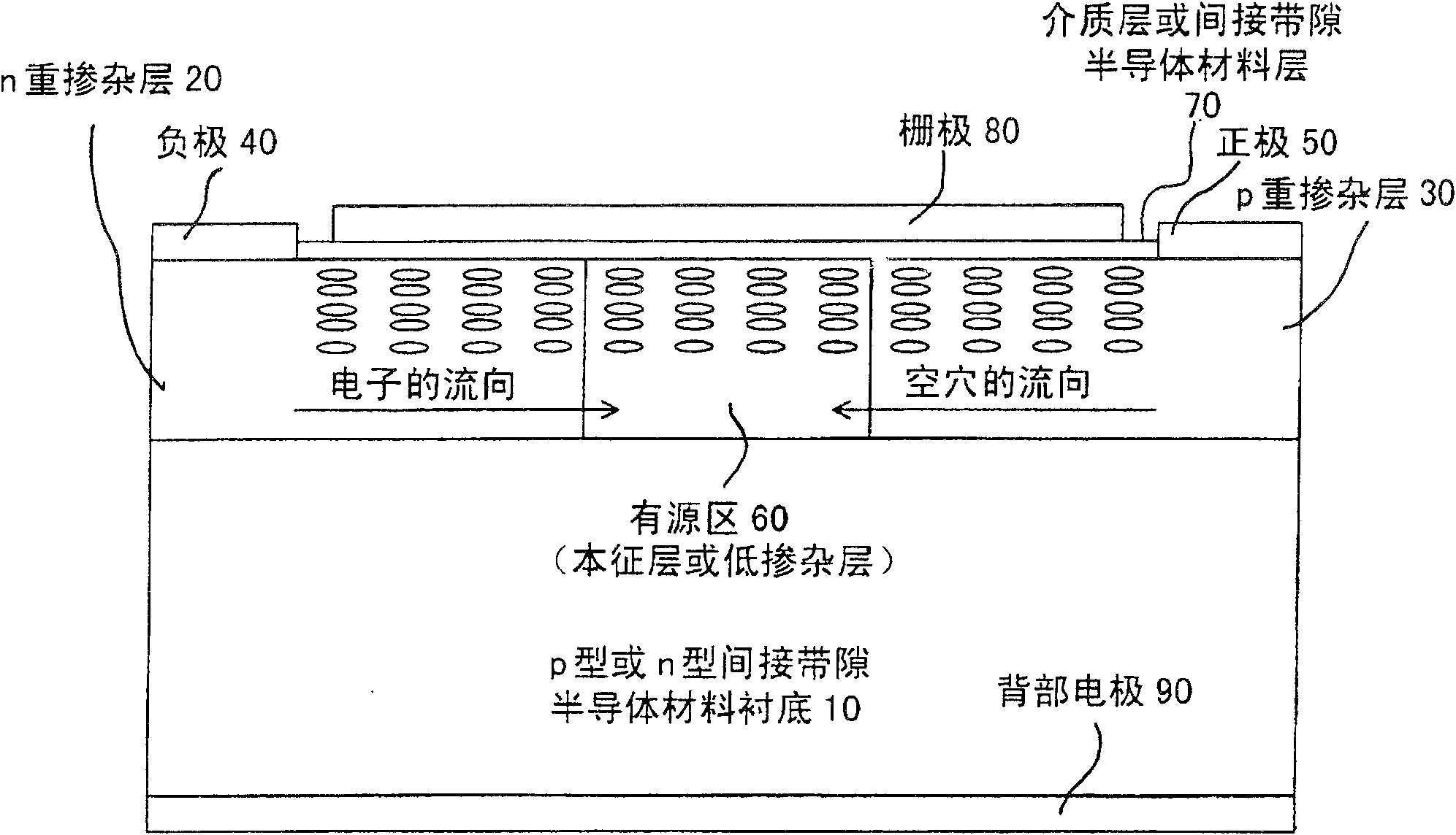
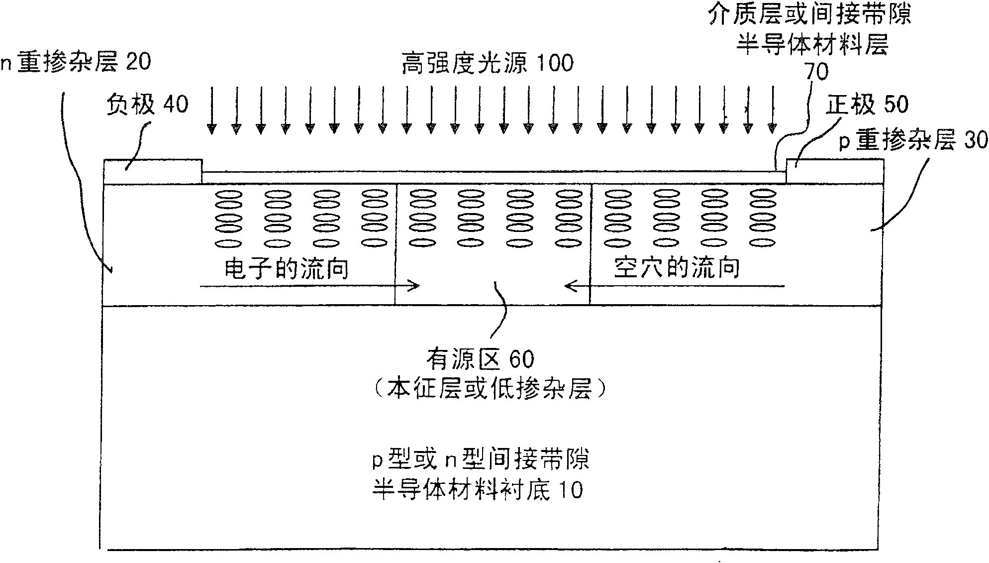
[0051] see Figure 1a As shown (it is the first embodiment of the present invention), a phonon-regulated indirect bandgap semiconductor material lateral electrical injection light-emitting device of the present invention is characterized in that it includes:

[0052] A p-type or n-type indirect bandgap semiconductor material substrate 10;

[0053] An n heavily doped layer 20, the n heavily doped layer 20 is made on one side of the p-type or n-type indirect bandgap semiconductor material substrate 10, and the n heavily doped layer 20 is the source region of the device;

[0054] A p heavily doped layer 30, the p heavily doped layer 30 is made on the other side of the p-type or n-type indirect bandgap semiconductor material substrate 10, the p heavily doped layer 30 is the drain region of the device ;

[0055] A negative electrode 40, the negative electrode 40 is made on the n heavily doped layer 20;

[0056] A positive electrode 50, the positive electrode 50 is made on the p h...


PUM


Abstract

A phonon-regulated indirect bandgap semiconductor material lateral electrical injection light-emitting device, comprising: a p-type or n-type indirect bandgap semiconductor material substrate; an n heavily doped layer made on one side of the substrate, the It is the source region of the device; a p heavily doped layer is made on the other side of the substrate, which is the drain region of the device; a negative electrode is made on the n heavily doped layer; a positive electrode is made on the p heavily doped layer; An active region is made in the middle of the substrate; a dielectric layer or an indirect band gap semiconductor material layer is made on the active region; a gate is made on the dielectric layer; a back electrode is made on the bottom of the substrate; The heavily doped layer, the p heavily doped layer and the active region are embedded with nanoscale silicon dioxide, silicon nitride, silicon oxynitride nanoparticles or nanoholes.

Description

technical field [0001] The invention relates to a lateral electrical injection light-emitting device of an indirect bandgap semiconductor material, in particular to a phonon-regulated lateral electrical injection light-emitting device of an indirect bandgap semiconductor material. Background technique [0002] Generally speaking, it is generally accepted that due to the indirect bandgap characteristics of indirect bandgap semiconductor materials, electrons and holes are not in the vertical direction of momentum space, and the luminescence transition requires the participation of phonons, which is a second-order and above process, and the efficiency is very low. Not suitable for consideration as a lighting system. However, it has been reported in the past that isoelectronic doping, such as nitrogen doping or zinc-oxygen pair doping, in indirect bandgap semiconductor materials such as gallium phosphide can achieve high-efficiency room-temperature emission of visible light and ...

Claims


Application Information

Patent Timeline
Patent Type & Authority Patents(China)
IPC IPC(8): H01L33/00
Inventor 张建国王晓欣成步文余金中王启明
Owner INST OF SEMICONDUCTORS - CHINESE ACAD OF SCI
Why Eureka
Try Eureka