
Method of inspecting an mura defect in a pattern and apparatus used for the same

A defect inspection and pattern technology, applied in the field of uneven pattern defect inspection devices, can solve the problems of deviation in inspection results, inability to detect with high precision, and difficulty in showing uneven defects, and achieve the effect of high precision detection

Inactive Publication Date: 2009-12-02
HOYA CORP
View PDF10 Cites 0 Cited by
  • Summary
  • Abstract
  • Description
  • Claims
  • Application Information

AI Technical Summary

Problems solved by technology

[0006] However, since this visual inspection has a problem that the inspection result varies depending on the operator, for example, an uneven defect inspection device such as Patent Document 1 has been proposed.
[0008] However, in the case of illuminating light sources such as fluorescent lamps and halogen lamps that irradiate non-directional diffuse light, the light cannot make the scattered light scattered at the edge of the unit pattern directional, and it comes from other parts other than the edge. The influence of reflected light, etc. increases, so uneven defects are difficult to appear
Therefore, there is a problem that unevenness defects cannot be detected with high accuracy in the conventional unevenness defect inspection device.

Method used


Image

  • Method of inspecting an mura defect in a pattern and apparatus used for the same
  • Method of inspecting an mura defect in a pattern and apparatus used for the same
  • Method of inspecting an mura defect in a pattern and apparatus used for the same

Examples


no. 2 Embodiment approach

[0050] [B] Second embodiment ( Figure 5 )

[0051] Figure 5 It is a perspective view showing a second embodiment of the pattern uneven defect inspection device of the present invention. In this second embodiment, the same reference numerals are attached to the same parts as those in the first embodiment described above, and description thereof will be omitted.

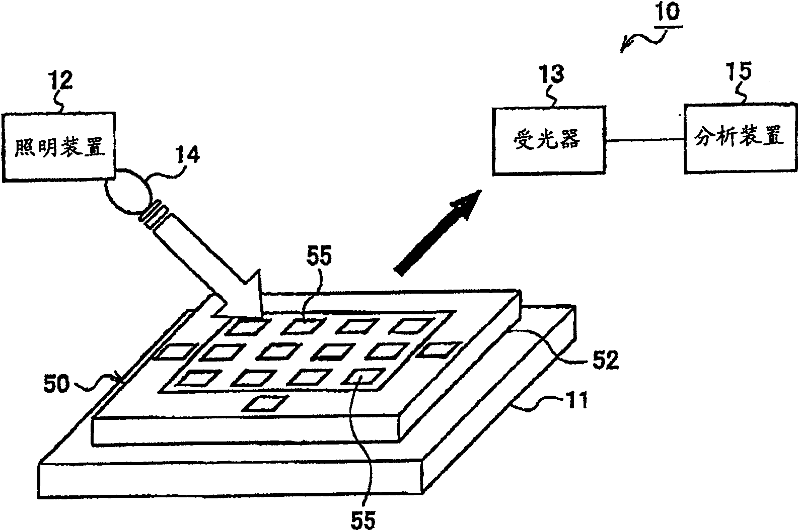
[0052] In the uneven defect inspection device 20 according to the second embodiment, the illuminating device 12 is disposed below the photomask 50 . Therefore, the photoreceiver 13 receives the transmitted light between the repeating patterns 51 in the chip 55 of the photomask 50 irradiated from the illuminating device 12 , especially the diffracted light diffracted at the edge of the unit pattern 55 in the transmitted light. , and converted into photometric data.

[0053]In this second embodiment, the illuminating device 12 directs the light emitted from the illuminating light source 16 with a directionality clo...


PUM


Abstract

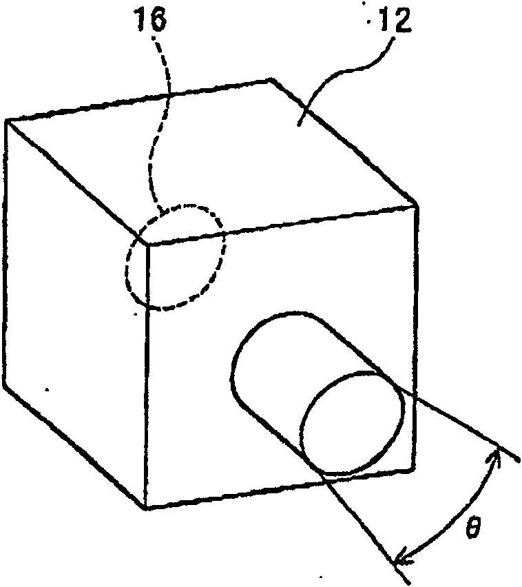
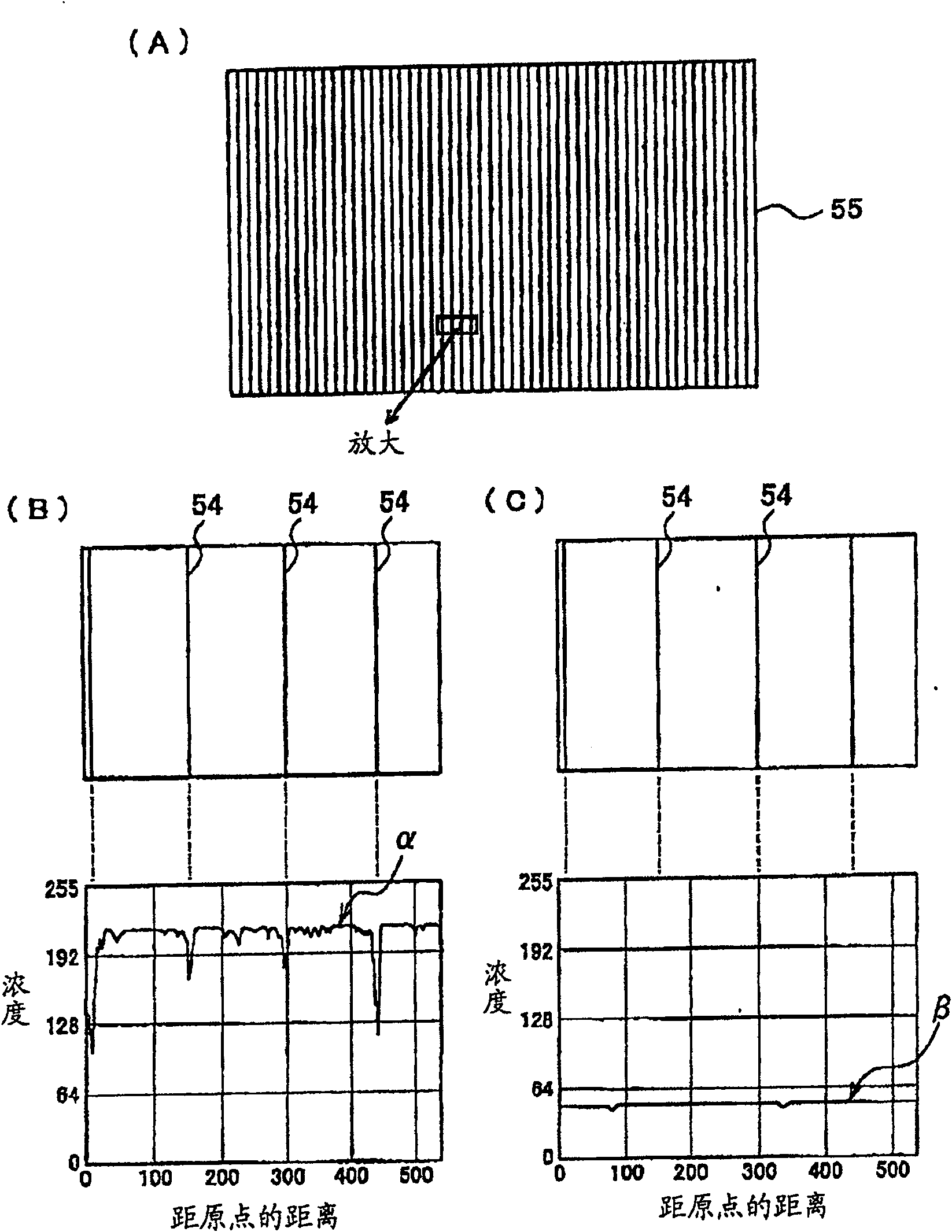
A mura defect inspection apparatus 10 having an illuminating unit 12 which irradiates light onto a photomask 50 having a chip 55 on the surface thereof, the chip is formed with a repeated pattern that a unit pattern is regularly arranged, and a photoreceptor 13 which receives scattered light generated at the edge part of the unit pattern of the repeated pattern on the chip of the photomask and converts it to received light data, wherein the received light data is analyzed to detect a mura defect generated in the repeated pattern, wherein the illuminating unit irradiates light that is emitted from an illumination light source and has a orientation property of the rays almost parallel, the light having a parallelism within an angle of 2°, for example, onto a repeated pattern 51 on the chip 55 of the photomask 50. This application claims foreign priority based on Japanese Patent application No. 2004 - 106462 , filed Mar. 31, 2004 , the contents of which is incorporated herein by reference in its entirety.

Description

technical field [0001] The present invention relates to a pattern uneven defect inspection method and a pattern uneven defect inspection device for detecting pattern uneven defects in video devices, or detecting pattern uneven defects in photomasks used for manufacturing patterns of video devices. Background technique [0002] Patent Document 1: Japanese Unexamined Patent Application Publication No. H10-300447 [0003] Conventionally, in video devices such as imaging devices and display devices, or photomasks used to manufacture these video devices, unevenness defect inspection has been used as an inspection item for patterns formed on the surface. Unevenness defects are errors with different regularities that unexpectedly occur in regularly arranged patterns, and occur due to certain reasons in the manufacturing process and the like. [0004] In an imaging device or a display device, if there is an unevenness defect, sensitivity unevenness and display unevenness may occur,...

Claims


Application Information

Patent Timeline
Patent Type & Authority Patents(China)
IPC IPC(8): G01N21/956G02F1/13G03F1/68G03F1/84G06K9/00
CPCG03F1/84G01N21/956A61H39/04A61H15/00A61H2205/125A61H2015/0014A61H2201/1253A61H2201/0192
Inventor 小林正明原督山口昇石川雄大
Owner HOYA CORP
Learn More