
Identical/symmetrical metal shielding

A related, photodetector technology, applied in the field of image sensors, which can solve problems affecting pixel performance

Active Publication Date: 2009-12-02
OMNIVISION TECH INC
View PDF4 Cites 0 Cited by
  • Summary
  • Abstract
  • Description
  • Claims
  • Application Information

AI Technical Summary

Problems solved by technology

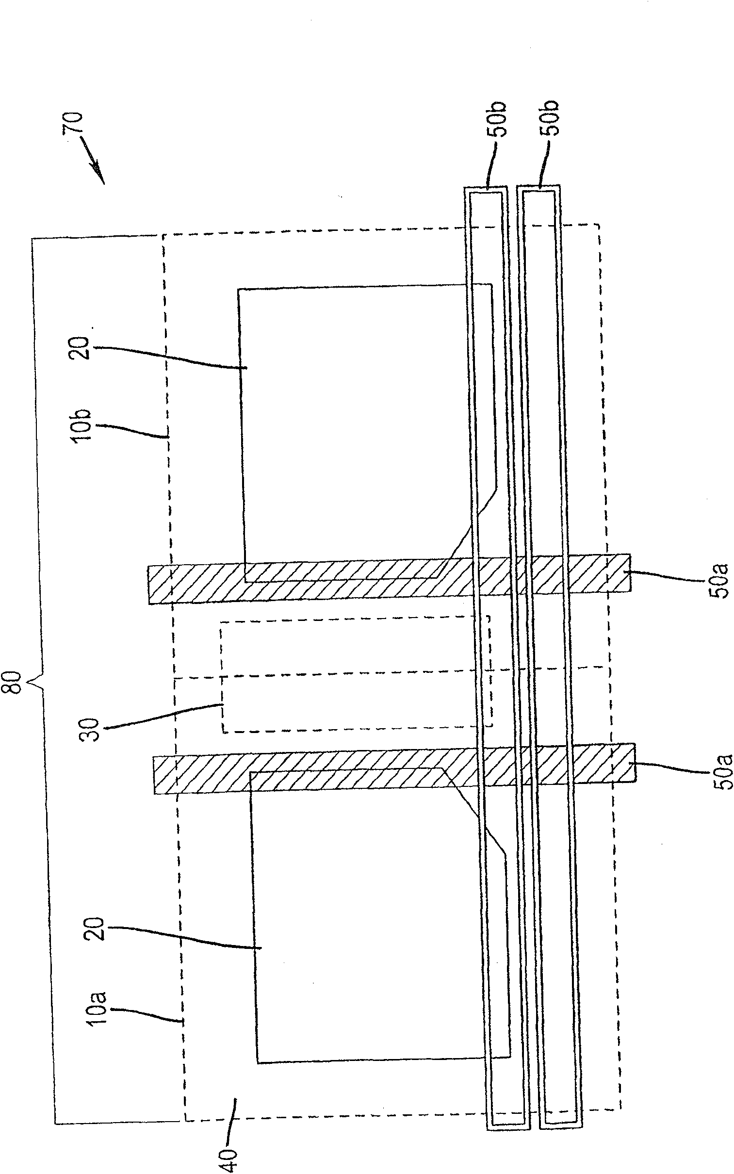
Assuming that the layout of the first pixel will be different from the layout of the second pixel due to the sharing of components, the misalignment of the photodiode 20 relative to the interconnection layer 50 will result in holes (by layers 50a, 50b and not covered by layer 50 The boundary definition of the photodiode 20) changes in size between the first pixel 10a and the second pixel 10b differently, which affects the pixel performance

Method used


Image

  • Identical/symmetrical metal shielding
  • Identical/symmetrical metal shielding
  • Identical/symmetrical metal shielding

Examples


Embodiment Construction

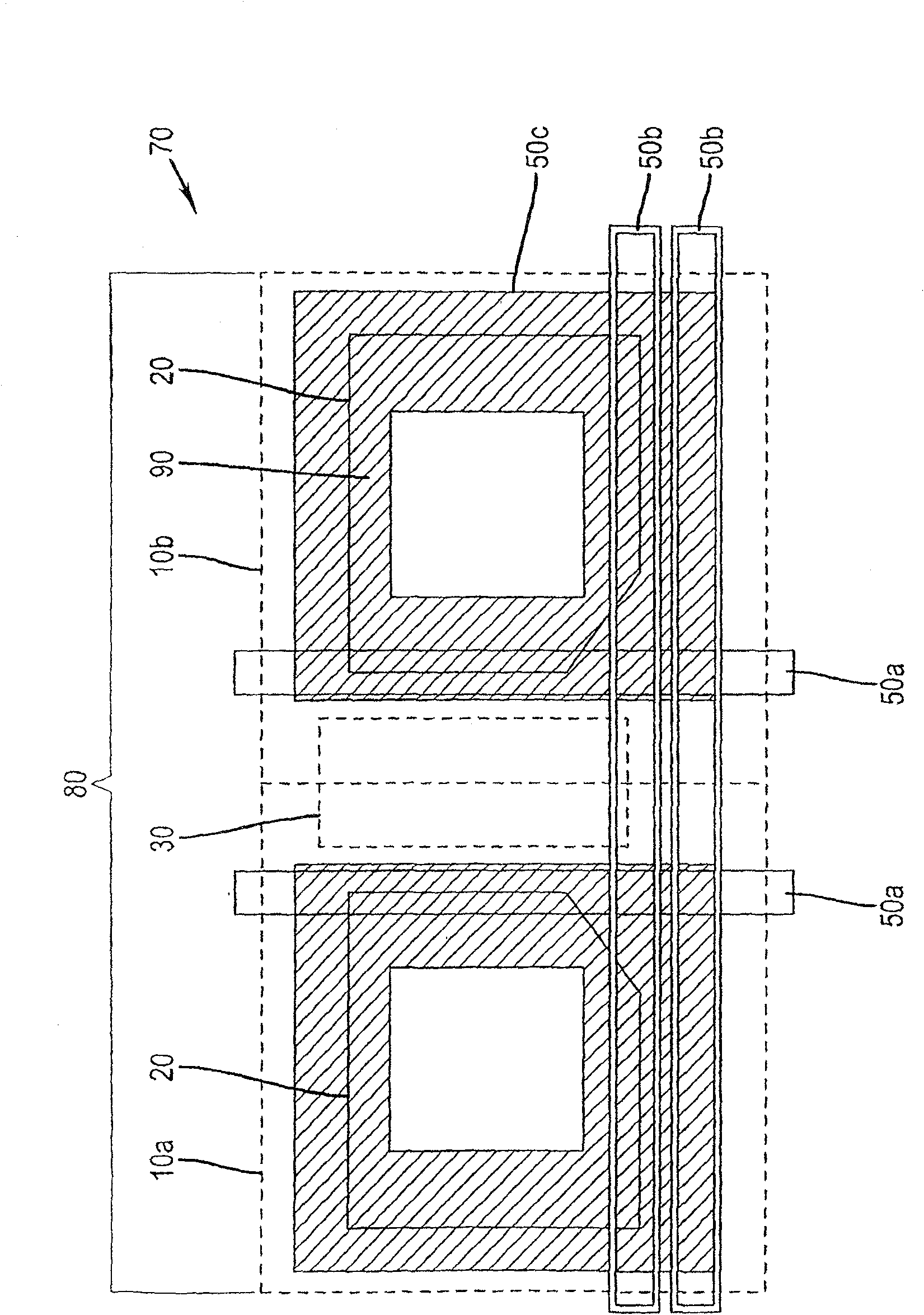
[0020] refer to Figure 4 , shows two photodiodes 100 of the image sensor 110 of the present invention. Each photodiode 100 accumulates charges in response to light. Photodiodes 100 are configured to be identical or substantially identical. There is a first interconnect layer 120a and a second interconnect layer 120b, which in combination form a light shield. It is instructive to note that preferably the first interconnection layer 120a and the second interconnection layer 120b are useful for more than light shielding. For example, they may be interconnected to provide bias or control clocks; to provide means for reading signals from pixels 130; or to provide pixels 130 or pixel superlattices (defined as elements in which there is a different shape but in the image local interconnect within two or more pixels with a repeating pattern on the sensor 110), where the pixel superlattice is not in Figure 4 shown in , while in Figure 5 , 7 and 9 are shown. The first intercon...


PUM


Abstract

An image sensor comprising a unit cell having a plurality of pixels; the unit cell comprising: a plurality of photodetectors having two or more subsets, wherein each subset has a different a physical shape; and an obscuring layer creating an aperture associated with each photodetector; wherein the obscuring layer is positioned such that any physical translation of the obscuring layer relative to the photodetector produces substantially equal The change.

Description

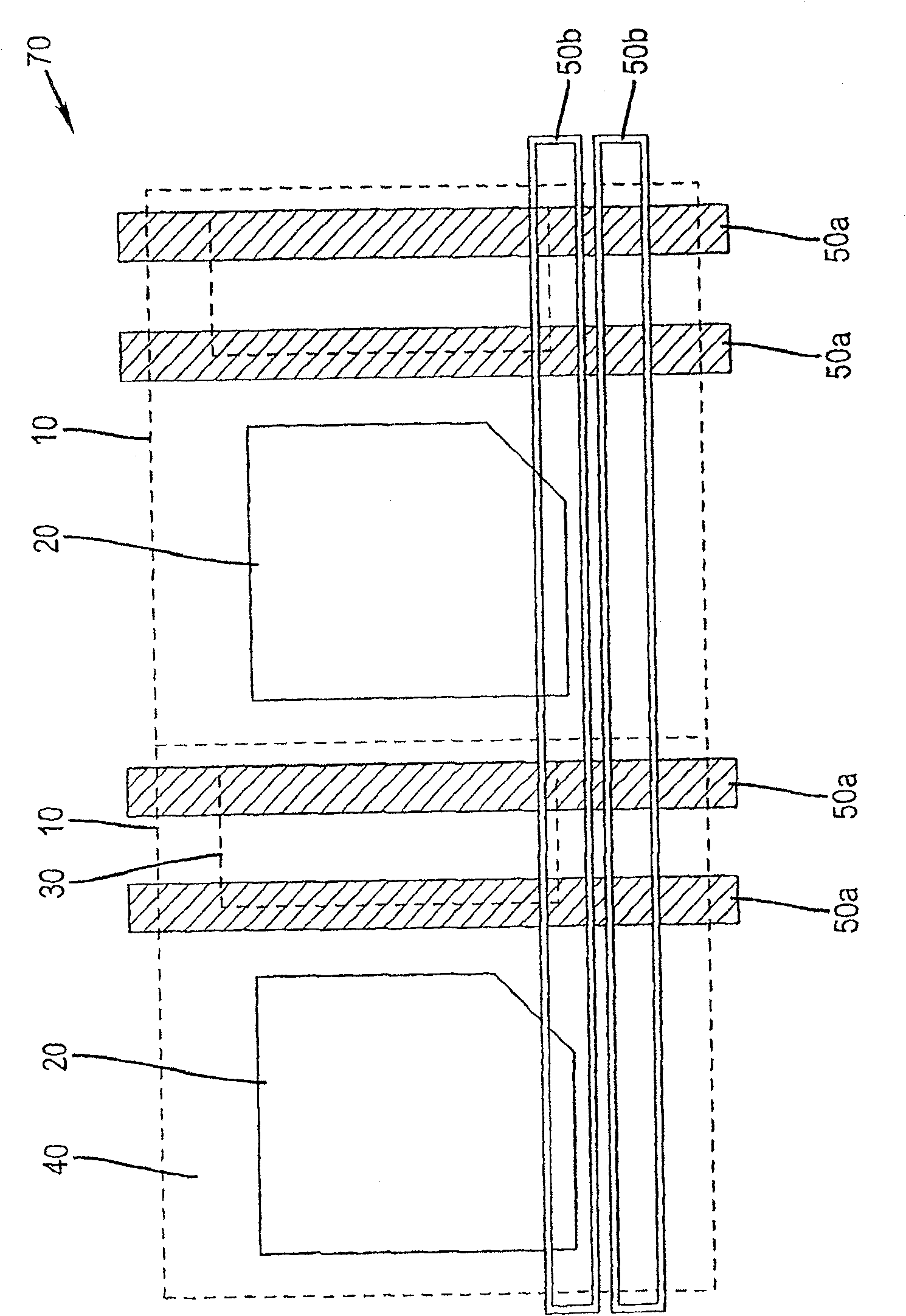
technical field [0001] The present invention relates generally to the field of image sensors, and more particularly, to an image sensor in which misalignment of a light shield does not change the size of the aperture. Background technique [0002] Referring to FIG. 1 , there is shown a prior art pixel 10 having a photodiode 20 , circuitry 30 , and isolation 40 and interconnect layers 50 . An interconnect layer is required to connect photodiodes 20 and circuitry 30 and to connect pixels 10 into pixel array 70 . The holes (defined by layers 50 a , 50 b and the boundaries of photodiodes 20 not covered by layer 50 b ) are set by the alignment of photodiodes 20 and interconnection layer 50 . Misalignment of the photodiode 20 relative to the interconnect layer 50 can cause the aperture to change size, which affects pixel performance. [0003] Referring to FIG. 2 , there is shown a prior art pixel supercell 80 consisting of a plurality of pixels 10 , such as a first pixel 10 a an...

Claims


Application Information

Patent Timeline
Patent Type & Authority Patents(China)
IPC IPC(8): H01L27/146
Inventor R·D·麦格拉思R·M·圭达什T·J·肯尼
Owner OMNIVISION TECH INC
Learn More