
Eureka
For R&D, Eureka makes reading and utilizing patents & technical documents easy.
Eureka AIR
Designed for self-driven R&D workflows. Generate viable solutions, solve complex R&D challenges, empower your innovation with AI.

Eureka Materials
Designed for material experts only. Revolutionize your material R&D, from search, analyze, to developing new materials.

TechResearch
Generate reliable direction feasibility study reports for your R&D in just a few steps.

TechSeek
Discover and master advanced knowledge NOW. Basics, ideas, possibilities, all at once.

TechMind
As an expert in R&D Theories, TechMind can generates customized viable solutions instantly.

TechRisk
Analyze your overall solution with one click, know your potential R&D risks in advance.

TechMonitor
Get weekly tech updates, stay abreast of the latest tech innovations and key insights.
Method for planarizing semiconductor structures
A semiconductor and planarization technology, used in semiconductor/solid-state device manufacturing, semiconductor/solid-state device testing/measurement, electrical components, etc., can solve problems such as reducing the grinding rate, and achieve the effect of reducing the step height difference
- Summary
- Abstract
- Description
- Claims
- Application Information
AI Technical Summary
Problems solved by technology
Method used
Image

Examples
Embodiment Construction
[0018] In order to make the above and other objects, features, and advantages of the present invention more obvious and understandable, a preferred embodiment, together with accompanying drawings, is described in detail as follows:
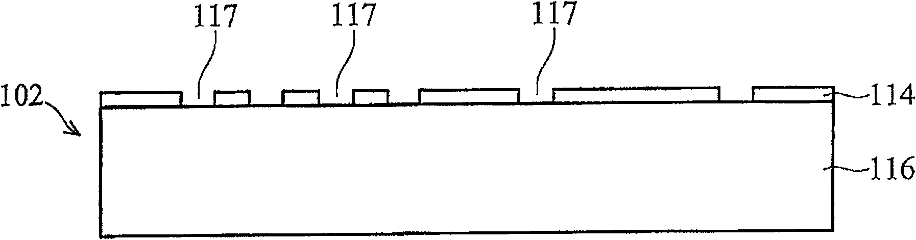
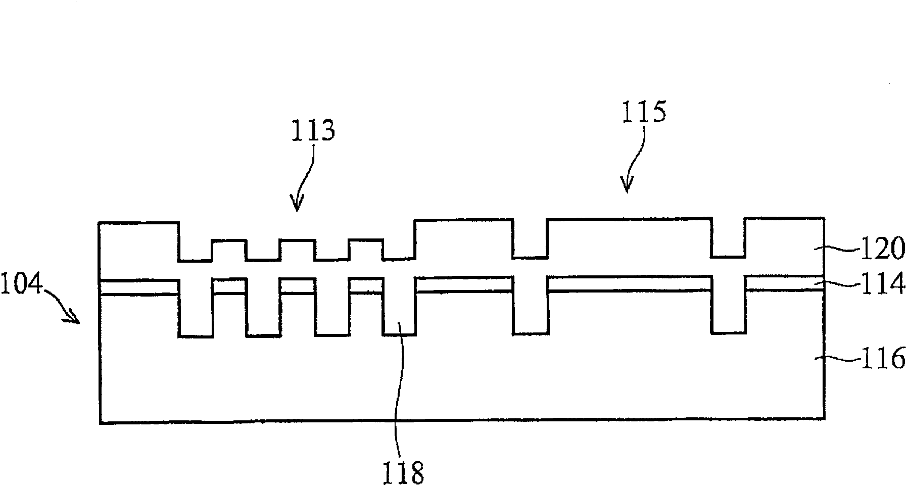
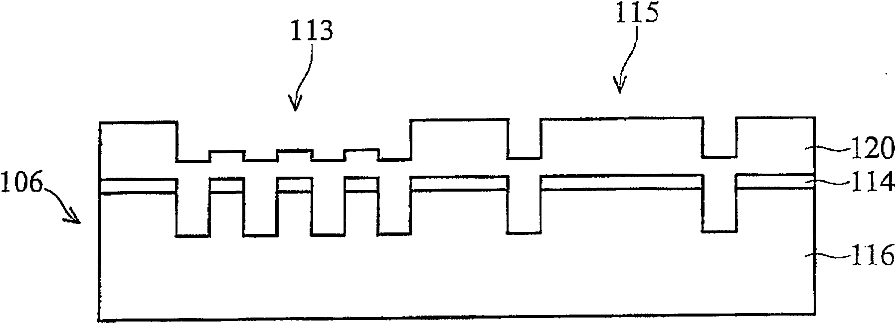
[0019] Figure 1A to Figure 1F Shows a cross-sectional view of the planarization process of the present invention. The method for planarizing a semiconductor structure of the present invention takes the formation of a shallow trench insulation structure (STI) as an example, but it can also be applied to the surface of various other semiconductor structures.
[0020] Figure 1A A cross-sectional view 102 showing the semiconductor structure includes a first dielectric layer 114 deposited on a semiconductor substrate 116. The first dielectric layer 114 can also be regarded as a barrier layer patterned by lithography technology, and has a plurality of openings for forming the shallow trench insulation structure. In this embodiment, the first dielectric lay...
PUM
| Property | Measurement | Unit |
|---|---|---|
| thickness | aaaaa | aaaaa |
| thickness | aaaaa | aaaaa |
Abstract
Description
Claims
Application Information
 - R&D Engineer
- R&D Manager
- IP Professional
- Industry Leading Data Capabilities
- Powerful AI technology
- Patent DNA Extraction
Browse by: Latest US Patents, China's latest patents, Technical Efficacy Thesaurus, Application Domain, Technology Topic, Popular Technical Reports.
© 2024 PatSnap. All rights reserved.Legal|Privacy policy|Modern Slavery Act Transparency Statement|Sitemap|About US| Contact US: help@patsnap.com