
Eureka
For R&D, Eureka makes reading and utilizing patents & technical documents easy.
Eureka AIR
Designed for self-driven R&D workflows. Generate viable solutions, solve complex R&D challenges, empower your innovation with AI.

Eureka Materials
Designed for material experts only. Revolutionize your material R&D, from search, analyze, to developing new materials.

TechResearch
Generate reliable direction feasibility study reports for your R&D in just a few steps.

TechSeek
Discover and master advanced knowledge NOW. Basics, ideas, possibilities, all at once.

TechMind
As an expert in R&D Theories, TechMind can generates customized viable solutions instantly.

TechRisk
Analyze your overall solution with one click, know your potential R&D risks in advance.

TechMonitor
Get weekly tech updates, stay abreast of the latest tech innovations and key insights.
Gate drive integrated circuit and forming method thereof
An integrated circuit and gate drive technology, applied in circuits, electrical components, semiconductor devices, etc., can solve the problems of high manufacturing cost, large chip size, and inability to reduce the size, and achieve low manufacturing cost, simplified manufacturing method, and reduced size. Effect
- Summary
- Abstract
- Description
- Claims
- Application Information
AI Technical Summary
Problems solved by technology
Method used
Image

Examples
Embodiment Construction
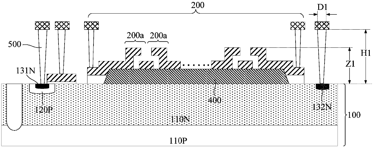
[0041] As mentioned in the background, in the existing gate drive integrated circuits, the field plate structure is a multi-level field plate structure, which not only has a high height, but also causes a gap between the top surface of the field plate structure and the substrate surface. The large step height difference, and the multi-level field plate structure generally needs to have a relatively large width dimension, which will lead to the inability to reduce the corresponding chip size and increase the manufacturing cost of the product.
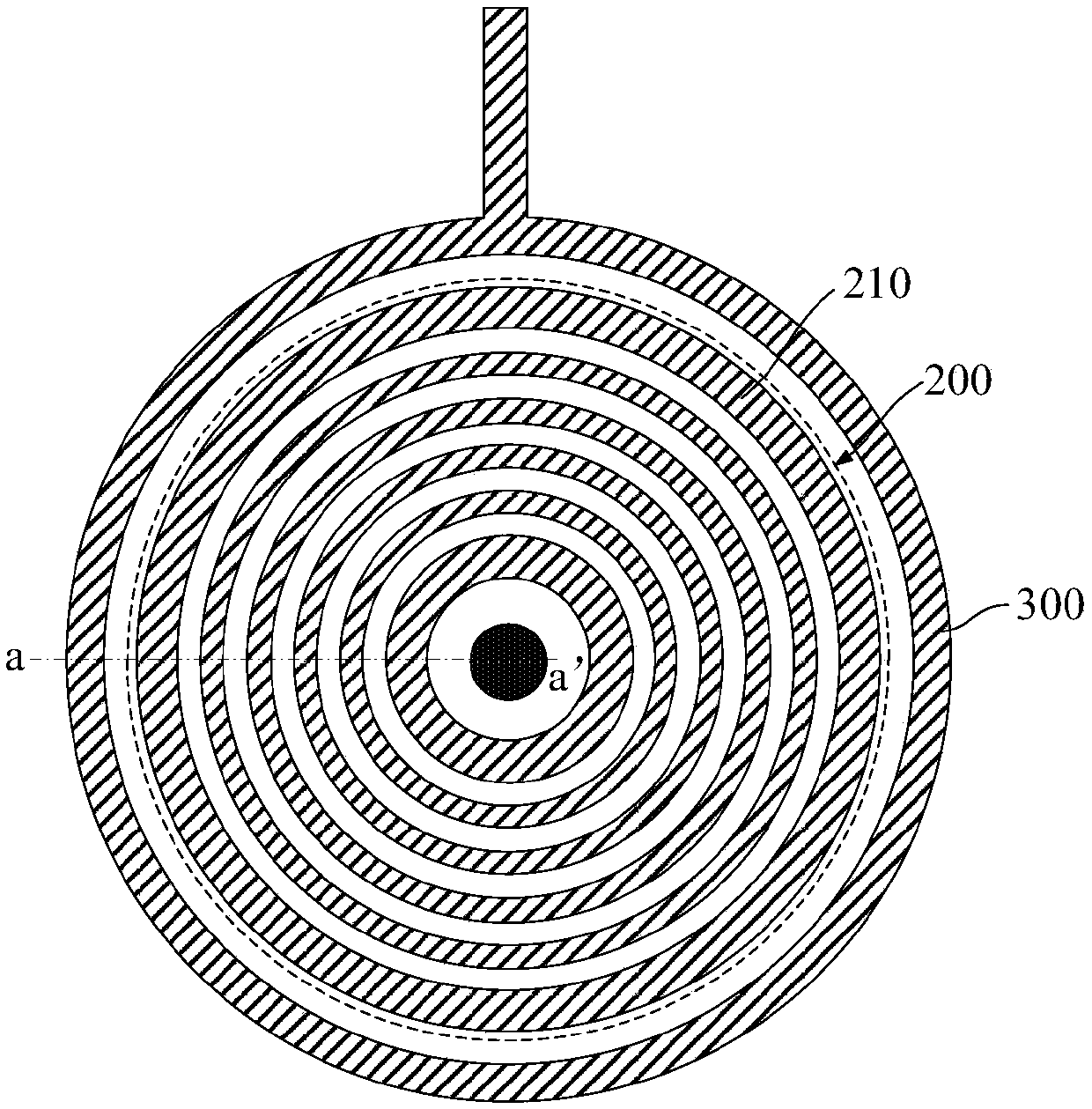
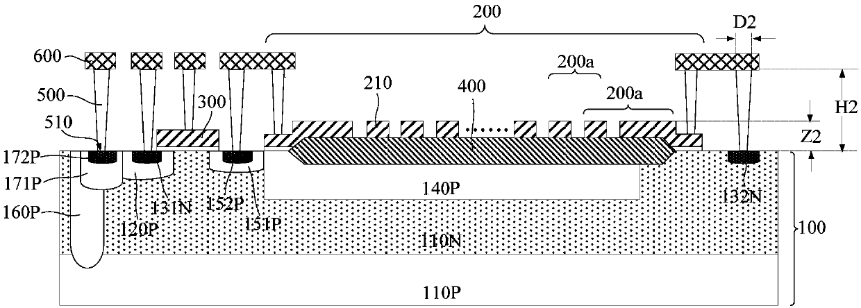
[0042] figure 1 It is a schematic structural diagram of a gate drive integrated circuit, such as figure 1 As shown, the gate drive integrated circuit includes:
[0043] A substrate 100, wherein a drift region 110N of a first doping type is formed in the substrate 100, and the drift region 110N extends from the top surface of the substrate to the interior of the substrate;
[0044] a field effect transistor, the field effect transistor ...
PUM
 Abstract
Description
Claims
Application Information
 - R&D Engineer
- R&D Manager
- IP Professional
- Industry Leading Data Capabilities
- Powerful AI technology
- Patent DNA Extraction
Browse by: Latest US Patents, China's latest patents, Technical Efficacy Thesaurus, Application Domain, Technology Topic, Popular Technical Reports.
© 2024 PatSnap. All rights reserved.Legal|Privacy policy|Modern Slavery Act Transparency Statement|Sitemap|About US| Contact US: help@patsnap.com