
Stacking encapsulation structure with symmetric multi-chip migration up and down

A stacking structure and packaging structure technology, applied in the direction of electrical components, electrical solid devices, circuits, etc., can solve the problems of different lengths of metal wires, uneven and uneven mold flow, phase changes of electrical signals, etc.

Active Publication Date: 2010-02-17
CHIPMOS TECH INC
View PDF2 Cites 0 Cited by
  • Summary
  • Abstract
  • Description
  • Claims
  • Application Information

AI Technical Summary

Problems solved by technology

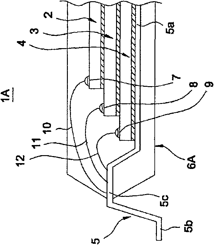
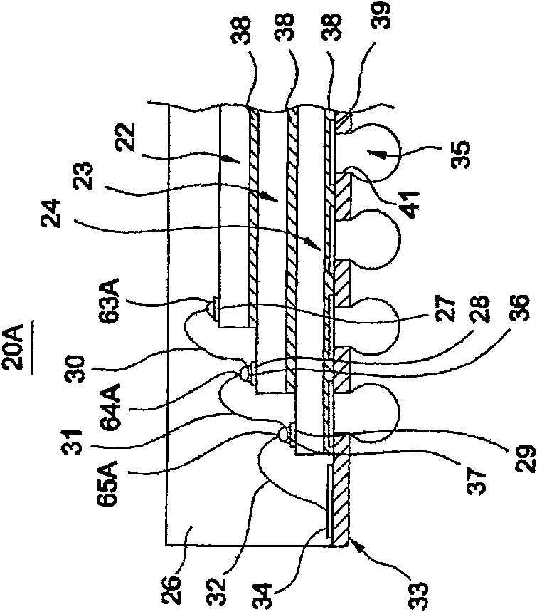
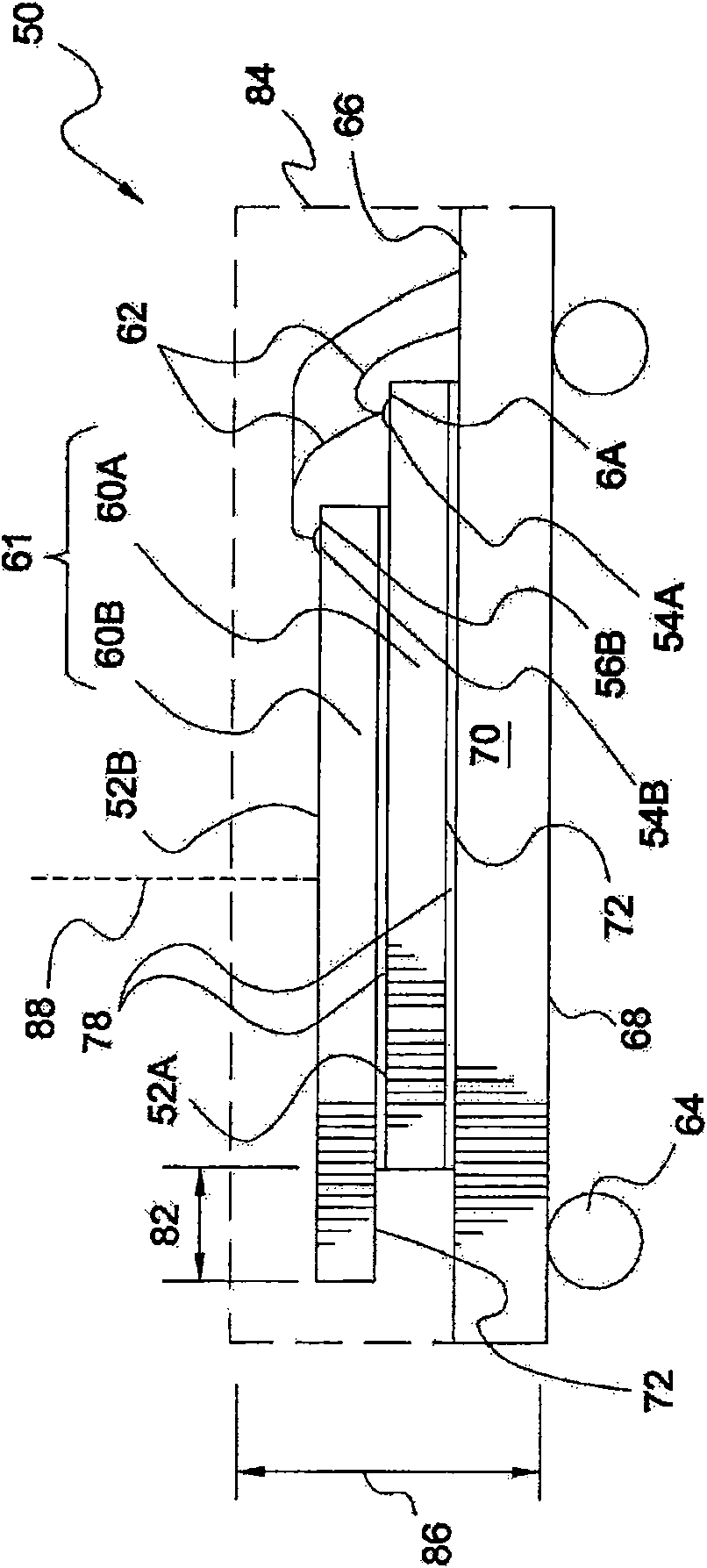
[0004] In the above-mentioned known chip stack package structure, in addition to the offset formed between the chips, which will cause uneven and uneven mold flow during injection molding; there are also metal wires between the chips, for example: Figure 1A 10, 11, 12 or Figure 1C In 62, the length and radian of each metal wire are different, so in addition to the metal wire with a longer length and radian during the sealing process, the metal wire with a longer length and radian is prone to displacement and cause a short circuit of the chip. The length is not the same, causing problems such as changes in the phase of the electrical signal

Method used


Image

  • Stacking encapsulation structure with symmetric multi-chip migration up and down
  • Stacking encapsulation structure with symmetric multi-chip migration up and down
  • Stacking encapsulation structure with symmetric multi-chip migration up and down

Examples


Embodiment approach

[0059] Please refer to Figure 2A and Figure 2B Shown is a schematic plan view and a schematic cross-sectional view of the chip 200 that has completed the aforementioned manufacturing process. like Figure 2B As shown, the chip 200 has an active surface 210 and a back surface 220 opposite to the active surface, and an adhesive layer 230 has been formed on the chip back surface 220; it should be emphasized here that the adhesive layer 230 of the present invention is not limited to the aforementioned prepreg The purpose of the adhesive layer 230 is to form a bond with the substrate or the chip. Therefore, as long as the adhesive material has this function, it is an embodiment of the present invention, such as a die attached film. In addition, the adhesive layer 230 of the present invention may also be formed of a material having an insulating function.

[0060] Next, please refer to Figure 2C , is a schematic cross-sectional view of a completed multi-chip offset stacking s...


PUM


Abstract

The invention provides a multi-chip offset stacked package structure, which is symmetric on upper and lower sides. The multi-chip offset stacked package structure comprises a wire holder composed of aplurality of inner pin groups that are oppositely arranged and a chip bearing seat, wherein the chip bearing seat is positioned among the plurality of inner pin groups, and both the inner pin groupsand the chip bearing seat have respective upper surfaces and low surfaces; a first multi-chip offset stacked package structure and a second multi-chip offset stacked package structure, which are respectively fixedly connected on the upper surface and the lower surface of the bearing seat of the chip; a plurality of metal wires for electronically connecting the first multi-chip offset stacked package structure and the second multi-chip offset stacked package structure with the inner pin groups; and a sealant for coating the first multi-chip offset stacked package structure, the second multi-chip offset stacked package structure, the inner pin groups and the bearing seat of the chip, and exposing outer pins.

Description

technical field [0001] The invention relates to a multi-chip stack package structure, in particular to a multi-chip offset stack package structure formed up and down symmetrically by chip holders. Background technique [0002] In recent years, three-dimensional (3D) packaging is being carried out in the back-end manufacturing process of semiconductors, hoping to use the least area to achieve higher density or memory capacity. In order to achieve this goal, a chip stacked method has been developed to achieve a three-dimensional (Three Dimension; 3D) package at this stage. [0003] In the known technology, the chip stacking method is to stack multiple chips on the substrate, and then use a wire bonding process to connect the multiple chips to the substrate. Figure 1A That is, a chip stack package structure based on a lead frame is disclosed, such as Figure 1A As shown, the lead frame 5 can be divided into an inner lead portion 5a, an outer lead portion 5b and a platform port...

Claims


Application Information

Patent Timeline
Patent Type & Authority Patents(China)
IPC IPC(8): H01L25/00H01L25/065H01L23/488H01L23/31
CPCH01L2224/32245H01L2924/15311H01L2224/73265H01L2224/48247H01L2224/32145H01L2224/48227H01L2224/32225H01L2225/06562H01L2224/48145H01L24/73H01L2924/181
Inventor 周世文陈煜仁
Owner CHIPMOS TECH INC
Learn More