Charge pumping circuit

A charge pump and circuit technology, applied in the direction of conversion equipment without intermediate conversion to AC, to achieve the effect of small ripple voltage and shorten the ripple period

Inactive Publication Date: 2007-10-03
ROHM CO LTD
View PDF1 Cites 9 Cited by
  • Summary
  • Abstract
  • Description
  • Claims
  • Application Information

AI Technical Summary

Problems solved by technology

Thus, no current flows through the OUT1 and OUT2 terminals of the current mirror circuit 120

Method used


Image

  • Charge pumping circuit
  • Charge pumping circuit
  • Charge pumping circuit

Examples


Embodiment Construction

[0045] Embodiments of the present invention will now be described with reference to the drawings. In the following description, the same or corresponding parts have the same reference numerals, and description thereof will not be repeated.

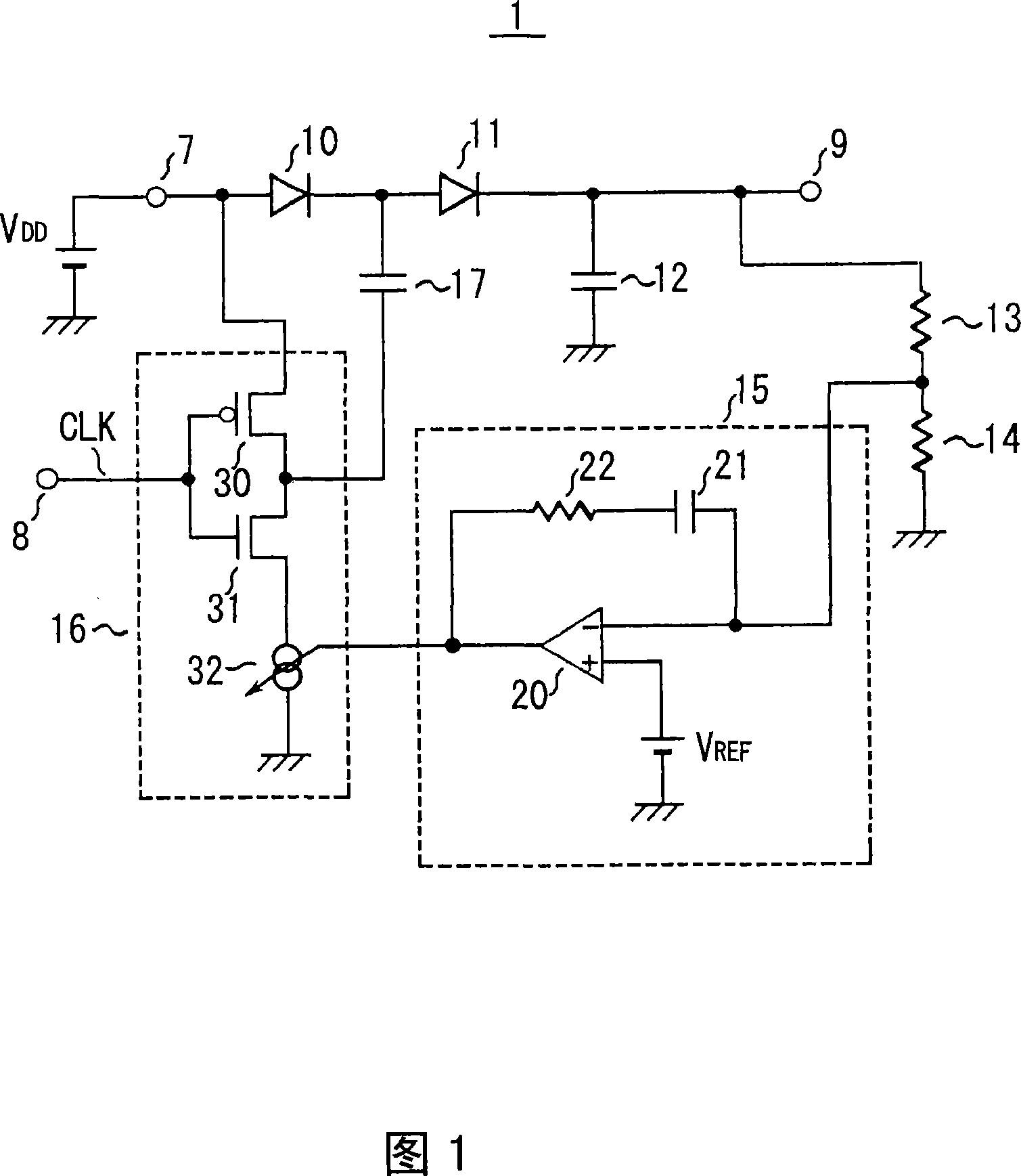
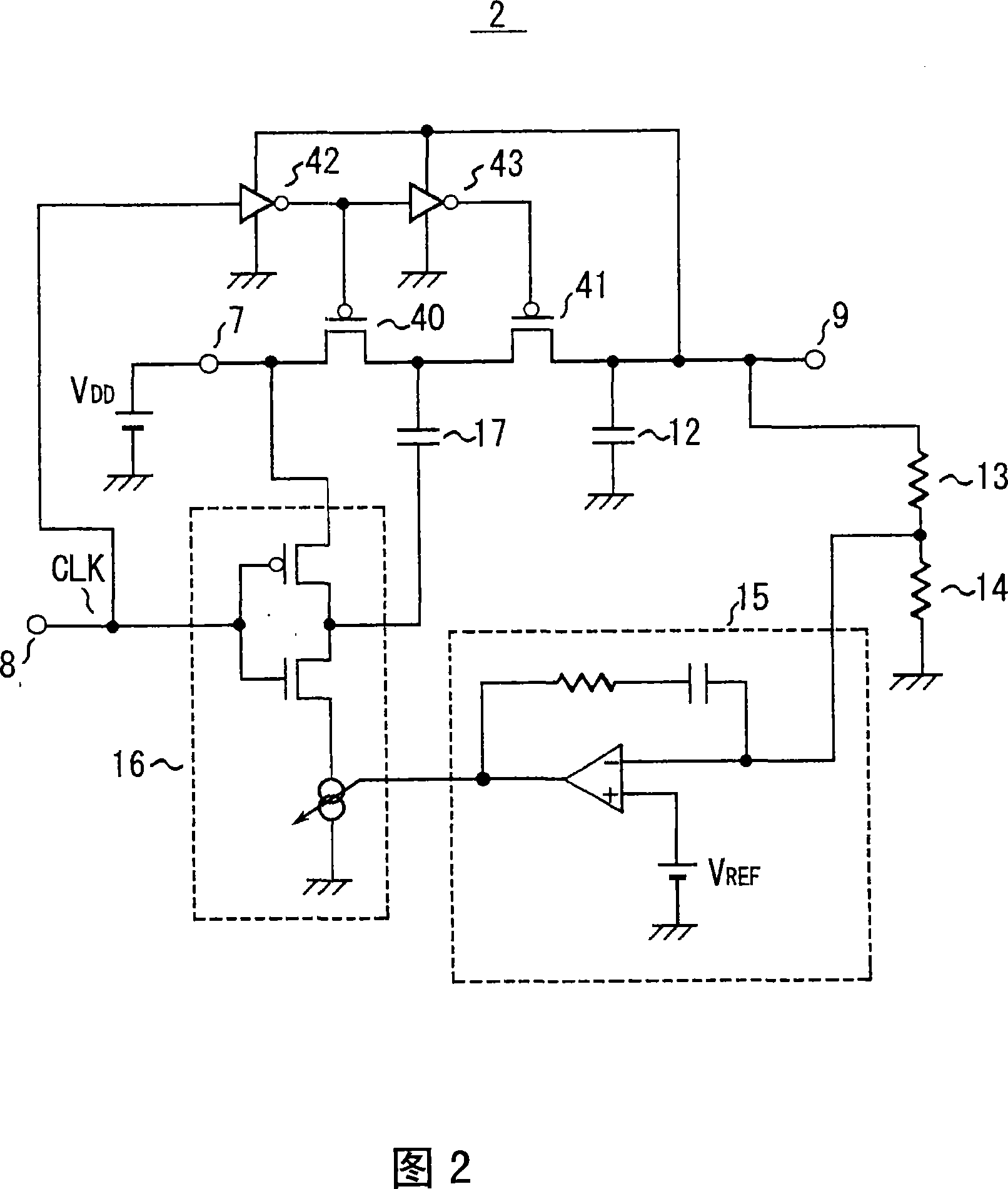
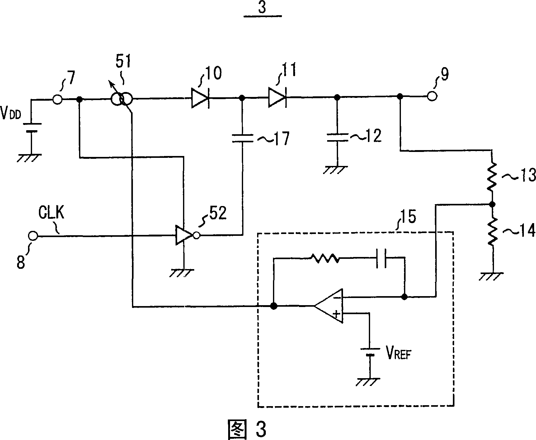
[0046] FIG. 1 is a circuit diagram of a charge pump circuit according to an embodiment of the present invention.

[0047] Referring to FIG. 1, a charge pump circuit 1 includes a receiving supply voltage V DD The input terminal 7 for receiving the clock signal CLK, the input terminal 8 for receiving the clock signal CLK, and the output terminal 9 for providing a predetermined boosted voltage to the load connected thereto.

[0048] First and second rectifying elements 10 and 11 , each being a diode element, are connected in series between the input and output terminals 7 and 9 . Although the diode elements shown in FIG. 1 are respectively PN junction diodes, MOS transistors whose gates and drains are connected together may be used. The ou...


PUM


Abstract

A charge pump circuit (1) comprising first and second rectification elements (10, 11) connected in series between an input terminal (7) and an output terminal (9) and outputting a predetermined voltage from the output terminal (9) when charges are moved sequentially through these rectification elements (10, 11) and stored in an output capacitor (12). The charge pump circuit (1) further comprises an integrator (15) for integrating the difference between a feedback voltage from the output terminal (9) and a reference voltage, a boost capacitor (17) having one end thereof connected with the joint point between the first and second rectification elements (10, 11), and a clock reverser (16) having power supply side and ground side transistors (30, 31) being inputted with a clock signal (CLK) and a variable current source (32) for feeding a current dependent on the output voltage from the integrator (15) to any one of the transistors, and having its output connected with the other end of the boost capacitor (17).

Description

technical field [0001] The present invention relates to a charge pump circuit for supplying a predetermined voltage. Background technique [0002] A charge pump circuit using a rectifying element such as a diode element or a switching element and a capacitor as main components has been widely used as a circuit that boosts an input voltage to provide a predetermined voltage. As one of such circuits, for example, in Japanese Patent Laid-Open No. 2000-066747 (Patent Document 1), a structure that performs feedback control to provide an appropriate output voltage has been proposed and disclosed. FIG. 5 shows a structure similar to that of the charge pump circuit disclosed in Patent Document 1. As shown in FIG. [0003] The charge pump circuit 101 has a receiving supply voltage V DD The input terminal 107 for receiving the clock signal CLK, the clock input terminal 108 for receiving the clock signal CLK, and the output terminal 109 for supplying a predetermined boosted voltage t...

Claims


Application Information

Patent Timeline
Patent Type & Authority Applications(China)
IPC IPC(8): H02M3/07
CPCH02M3/07
Inventor 中田健一
Owner ROHM CO LTD
Why Eureka
Try Eureka