Charge pump circuit

A charge pump and circuit technology, applied in the direction of conversion equipment without intermediate conversion to AC, can solve the problem of increasing the output jitter of the phase-locked loop circuit, and achieve the effect of improving the output noise performance and reducing the ripple voltage

Inactive Publication Date: 2011-04-20
SHANGHAI INTEGRATED CIRCUIT RES & DEV CENT
View PDF5 Cites 9 Cited by
  • Summary
  • Abstract
  • Description
  • Claims
  • Application Information

AI Technical Summary

Problems solved by technology

[0004] In order to overcome the current mismatch between the charge pump circuit NMOS and the PMOS current mirror that exists in the above-mentioned prior art, causing ripples on the output voltage, thereby increasing the output jitter problem of the phase-locked loop circuit, the main purpose of the present invention is to provide a The charge pump circuit used in the phase-locked loop circuit, through the feedback effect of the reference voltage negative feedback circuit on the differential complementary MOS switch, makes the currents flowing through the complementary two sets of differential MOS switches fully match, effectively reducing the current caused by the current source. The ripple voltage caused by the mismatch at the output voltage terminal greatly improves the output noise performance of the PLL circuit

Method used


Image

  • Charge pump circuit
  • Charge pump circuit
  • Charge pump circuit

Examples


Embodiment Construction

[0020] In order to make the content of the present invention clearer and easier to understand, the content of the present invention will be described in detail below in conjunction with specific embodiments and accompanying drawings.

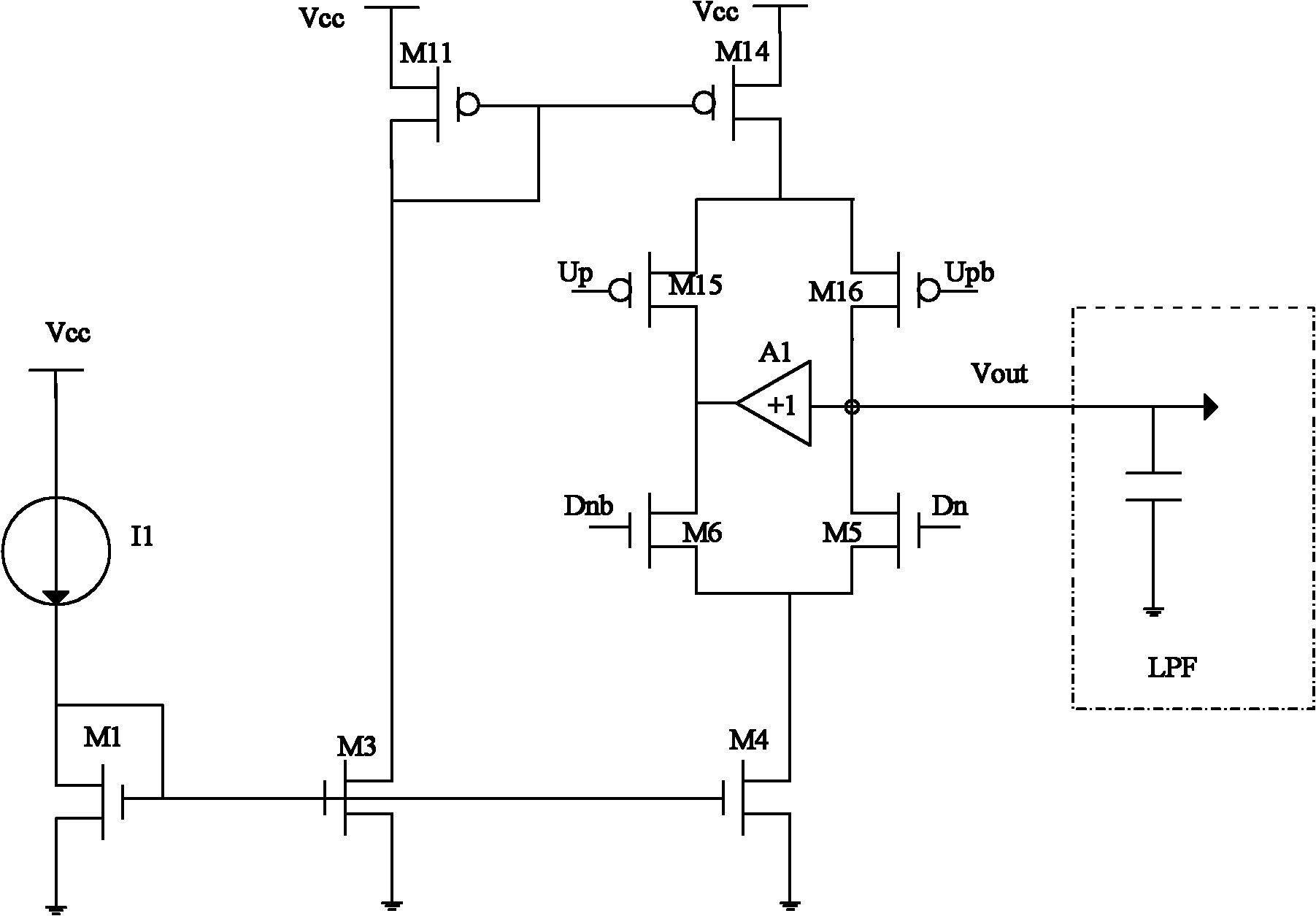
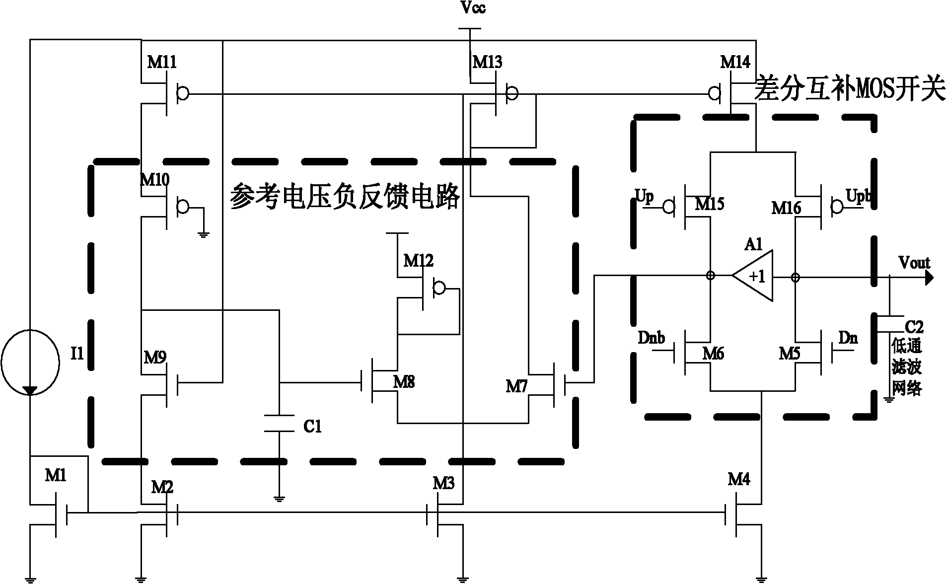
[0021] figure 2 is a circuit structure diagram of a charge pump circuit according to an embodiment of the present invention. figure 2 The charge pump circuit shown can be arranged in a phase locked loop circuit.

[0022] figure 2 The shown charge pump circuit that can be arranged in a phase-locked loop circuit according to an embodiment of the present invention includes: a set of NMOS differential pair transistors, a set of PMOS differential pair transistors, and a differential complementary MOS switch composed of a unity gain amplifier; A set of PMOS current mirrors; a set of NMOS current mirrors; a set of reference voltage negative feedback circuits. The present invention uses the feedback effect of the reference voltage negative feedbac...


PUM


Abstract

The invention provides a charge pump circuit. The charge pump circuit comprises a group of differential complementary metal-oxide-semiconductor (MOS) switch circuits, a reference voltage negative feedback circuit, a group of N-channel metal-oxide-semiconductor (NMOS) current mirrors and a group of P-channel metal-oxide-semiconductor (PMOS) current mirrors, wherein the group of NMOS current mirrors and the group of PMOS current mirrors are respectively connected to the differential complementary MOS switch circuits and the reference voltage negative feedback circuit for providing mirror currents; and the reference voltage negative feedback circuit is connected with differential complementary MOS switches, so that the reference voltage negative feedback circuit provides feedback for the differential complementary MOS switches. Currents flowing through two groups of complementary differential MOS switches are completely matched through the feedback action of the reference voltage negative feedback circuit on the differential complementary MOS switches, so that the ripple voltage generated at an output voltage end due to unmatched current sources is effectively reduced, and the output noise performance of a phase locked loop is greatly improved.

Description

technical field [0001] The invention relates to a charge pump circuit, in particular to a charge pump circuit arranged in a phase-locked loop circuit. Background technique [0002] figure 1 It is a structural schematic diagram of a charge pump circuit commonly used in a phase-locked loop circuit in the prior art. Such as figure 1 As shown, M5 / M6 / M15 / M16 in the figure are MOS switches, Up / Upb, Dn / Dnb come from two pairs of differential signals output by the frequency and phase detector. Reference numeral A1 denotes a unity gain amplifier, which functions to cancel charge sharing. In the phase-locked loop circuit design, the output voltage Vout of the charge pump is a very critical design factor. [0003] exist figure 1 In the traditional charge pump shown, if the currents generated by the NMOS and PMOS current mirrors do not match, ripples will be caused on the output voltage terminal Vout, thereby increasing the output jitter of the phase-locked loop circuit. Contents...

Claims


Application Information

Patent Timeline
Patent Type & Authority Applications(China)
IPC IPC(8): H02M3/07
Inventor 任铮
Owner SHANGHAI INTEGRATED CIRCUIT RES & DEV CENT
Why Eureka
Try Eureka