Succesive approximation type analogue-digital converting circuit

A successive approximation and capacitive technology, applied in analog-to-digital converters, analog-to-digital conversion, code conversion, etc., can solve the problems of voltage calibration sub-circuits without correction function, increased power consumption, complex circuits, etc., to achieve functional The effect of low power consumption, elimination of mismatch error, and compact structure

CN101072032AActive Publication Date: 2007-11-14SANECHIPS TECH CO LTD
1 Cites 21 Cited by

Patent Information

Authority / Receiving Office
CN · China
Patent Type
Applications(China)
Current Assignee / Owner
Publication Date
2007-11-14

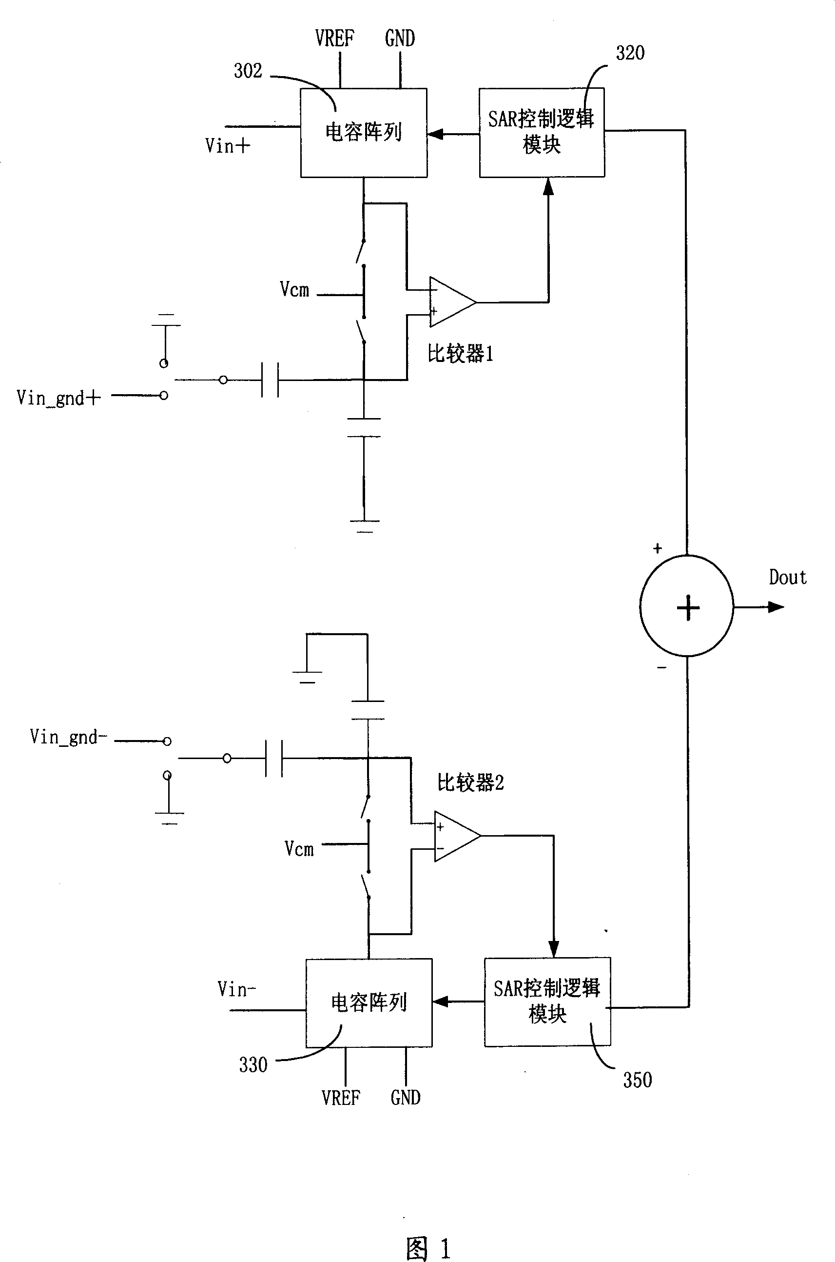
Smart Images

  • Figure 1
    Figure 1
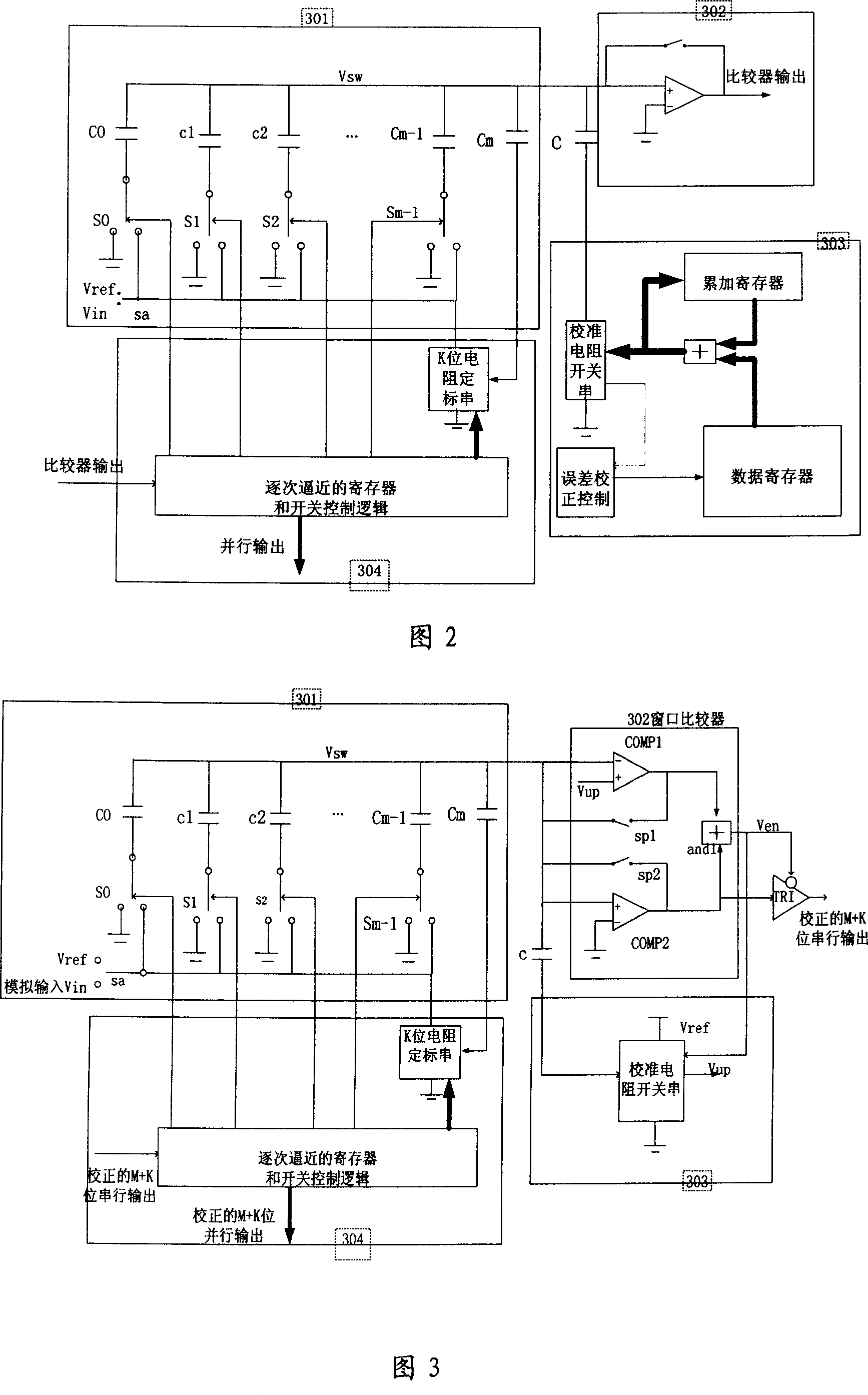
  • Figure 2
    Figure 2
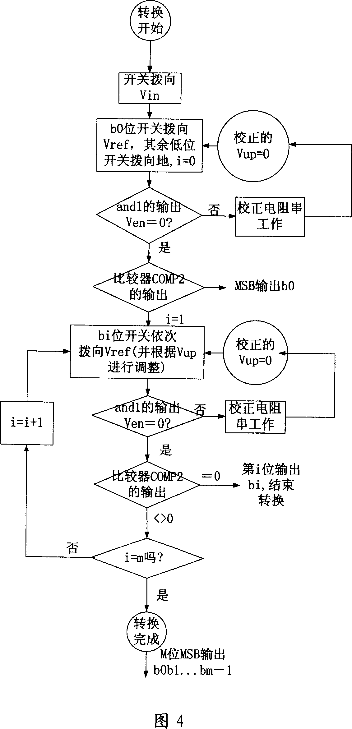
  • Figure 3
    Figure 3
Patent Text Reader

Abstract

The comparator module is a window comparator (WC). WC includes a first comparator (FC), second comparator (SC) and a pair of switch. FC carries out comparison between the output signal and a reference signal once. Negative end of FC and positive end of SC are connected to the switching signals of the capacitance and the switch array. Positive end of FC is connected to the reference signal, and the negative end of SC is connected to ground signal. FC and SC carry out comparison between the output signal and ground signal once respectively. Result signal is obtained by AND operation for the two compared results. The higher signal in result signals is the result caused by mismatched error (ME) of charge calibration. Feeding back ME to the correction resistance switches, the sequential approximation register, and the switch control logic module to correct the output of WC to zero. Eliminating ME, the invention possesses features of fine structure, and lower power consumption.
Need to check novelty before this filing date? Find Prior Art

Description

technical field

[0001] The present invention relates to a successive approximation (SAR) analog-to-digital conversion circuit (ADC), in particular to a charge-scaling and voltage-scaling successive approximation model with error correction Microelectronic circuit for digital conversion. Background technique

[0002] The successive approximation A / D converter has become one of the most commonly used methods of A / D conversion due to its reasonably fast conversion time and moderate circuit complexity.

[0003] The successive approximation A / D converter is divided into two main commonly used forms: voltage calibration first followed by charge calibration and charge calibration followed by voltage calibration. Here, voltage calibration is a module structured by the distribution of resistor switch strings. Charge calibration is a module with a switched capacitor array structure. The reason why a single resistive switch module or switched capacitor module is not used is to avoid a...

Examples

Embodiment Construction

[0028] Below in conjunction with the accompanying drawings, the method of the present invention will be further described in detail.

[0029] The analog-to-digital conversion circuit of successive approximation of the present invention, as shown in Figure 3, on the basis of the circuit in Figure 2 of the prior art, at first module 202 is transformed into a window comparator 302, and the window comparator includes the first comparator COMP1 and the second comparator Two comparators COMP2 and a pair of switches sp1, sp2, the first comparator COMP1 compares the output signal with the reference signal Vup once, the negative terminal of the first comparator COMP1 and the positive terminal of the second comparator COMP2 are connected to the 301 module ( That is, the switching signal Vsw signal of the switch array 201) in the prior art, the positive terminal of the first comparator COMP1 is connected to the Vup signal, the negative terminal of the second comparator COMP2 is grounded, ...