

Printed circuit board and manufacturing method thereof
A wiring circuit board and a manufacturing method technology, applied in the direction of printed circuit manufacturing, printed circuit, printed circuit, etc., can solve the problem of failure to improve the bonding performance of the conductor pattern and the covering insulating layer, the length of the transmission path becomes longer, and the transmission characteristics deteriorate, etc. question
- Summary
- Abstract
- Description
- Claims
- Application Information
AI Technical Summary
Problems solved by technology
Method used
Image

Examples
no. 1 approach
[0055] First, the overall configuration of the printed circuit board of the present embodiment and the second to fourth embodiments described later will be described.
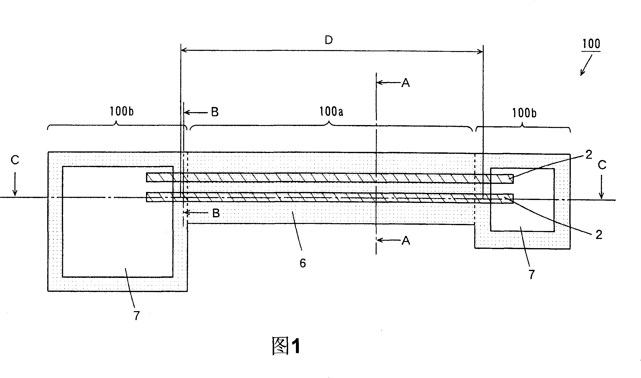
[0056] FIG. 1 is a perspective view showing the overall configuration of a printed circuit board according to the first to fourth embodiments.
[0057] As shown in FIG. 1 , printed circuit board 100 of the present embodiment has bent portion 100 a bent during use and non-bent portion 100 b not bent during use. In the present embodiment, the curved portion 100a is provided between the two non-bent portions 100b having different sizes.
[0058] The bent portion 100a is a bent portion or a repeatedly bent portion, and the non-bent portion 100b is a portion mounted on a semiconductor chip or the like without bending.
[0059] A plurality of (two in this embodiment) conductor patterns 2 are formed substantially parallel to the outer shape of the curved portion 100a from one non-bent portion 100b to the other non-be...
no. 2 approach
[0083] Next, a method of manufacturing printed circuit board 100 according to the second embodiment will be described.
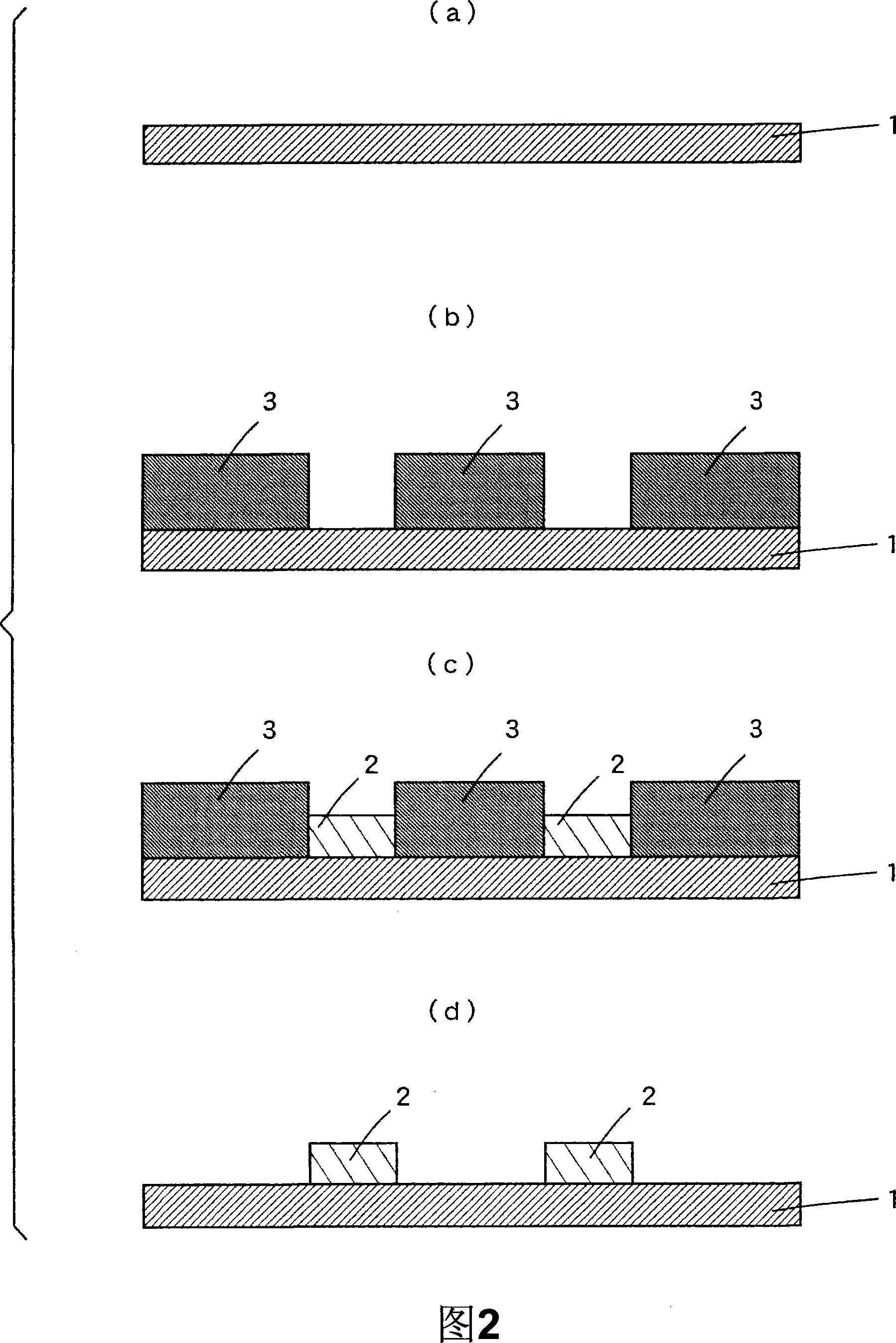
[0084] In the second embodiment, since the steps up to forming the predetermined conductive pattern 2 on the insulating base layer 1 by the semi-additive method are the same as those of the first embodiment (the steps corresponding to FIGS. 2(a) to (d)), Its description is omitted.
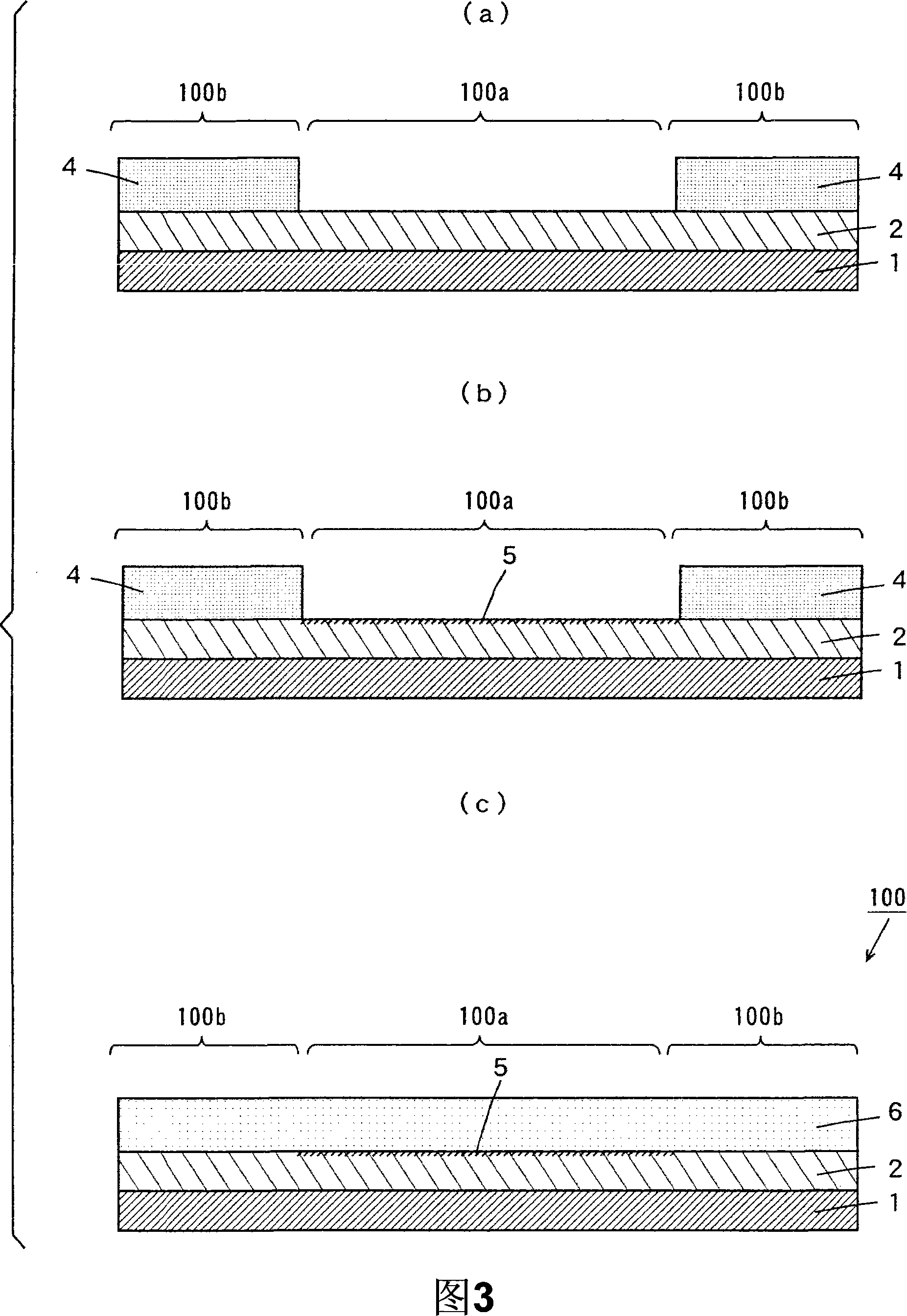
[0085]FIG. 5 is a cross-sectional view showing another example of the steps from forming the conductive pattern 2 on the insulating base layer 1 to manufacturing the printed circuit board 100 . 5 shows a region D in the C-C line cross-section of printed circuit board 100 in FIG. 1 .
[0086] On the insulating base layer 1, a predetermined conductor pattern 2 is formed across the bent portion 100a and the two non-bent portions 100b. In this way, the member in which the conductive pattern 2 is formed on the insulating base layer 1 is immersed in the same treatment liquid for rou...
no. 3 approach
[0094] Next, a method of manufacturing printed circuit board 100 according to the third embodiment will be described.
[0095] In the third embodiment, after the plating resist layer 3 is formed on the insulating base layer 1, the process of forming the conductive pattern 2 on the surface of the insulating base layer 1 on which the plating resist layer 3 is not formed is different from the first Embodiment (the process corresponding to FIG.2(a)-(c)) is the same, and the description is abbreviate|omitted. Therefore, the steps from the step of FIG. 2( c ) to the manufacturing of the printed circuit board 100 of this embodiment will be described below.
[0096] FIGS. 6A and 6B are cross-sectional views showing other examples of each process from the process of FIG. 2( c ) to the production of the printed circuit board 100 .
[0097] Wherein in Fig. 6A and Fig. 6B, (A1) and (B1), (A2) and (B2), (A3) and (B3) and (A4) and (B4) respectively represent the section of different region...
PUM
 Abstract
Description
Claims
Application Information