Printed circuit board unit

A technology of printed circuit boards and printed circuit boards, which is applied in the direction of printed circuits, printed circuits, printed circuit manufacturing, etc., and can solve the problems of time-consuming bending of wires and increased production costs

Inactive Publication Date: 2007-11-28
FUJITSU LTD
View PDF1 Cites 14 Cited by
  • Summary
  • Abstract
  • Description
  • Claims
  • Application Information

AI Technical Summary

Problems solved by technology

Variations in the design of standard products lead to increased production costs
Also, bending wires is time consuming

Method used


Image

  • Printed circuit board unit
  • Printed circuit board unit
  • Printed circuit board unit

Examples


Embodiment Construction

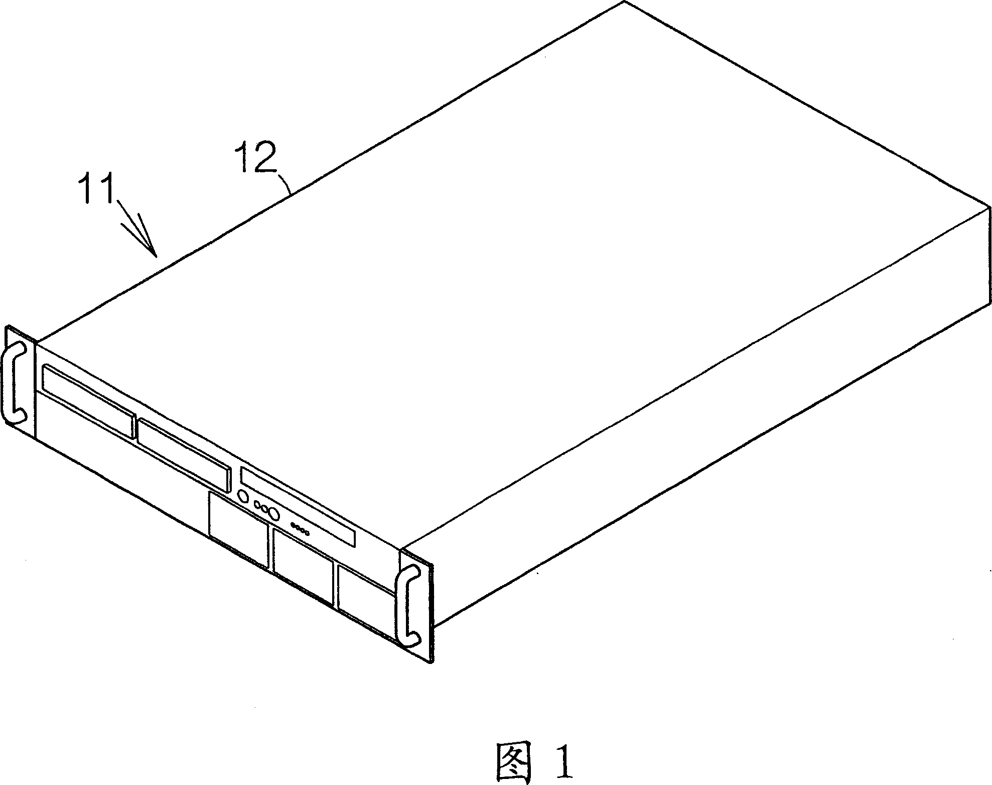
[0029] FIG. 1 schematically shows a server computer 11 as a specific example of electronic equipment according to an embodiment of the present invention. The server computer 11 is mounted on a rack, for example. The server computer 11 includes a housing 12 . A printed circuit board unit or motherboard unit is housed within the housing 12 .

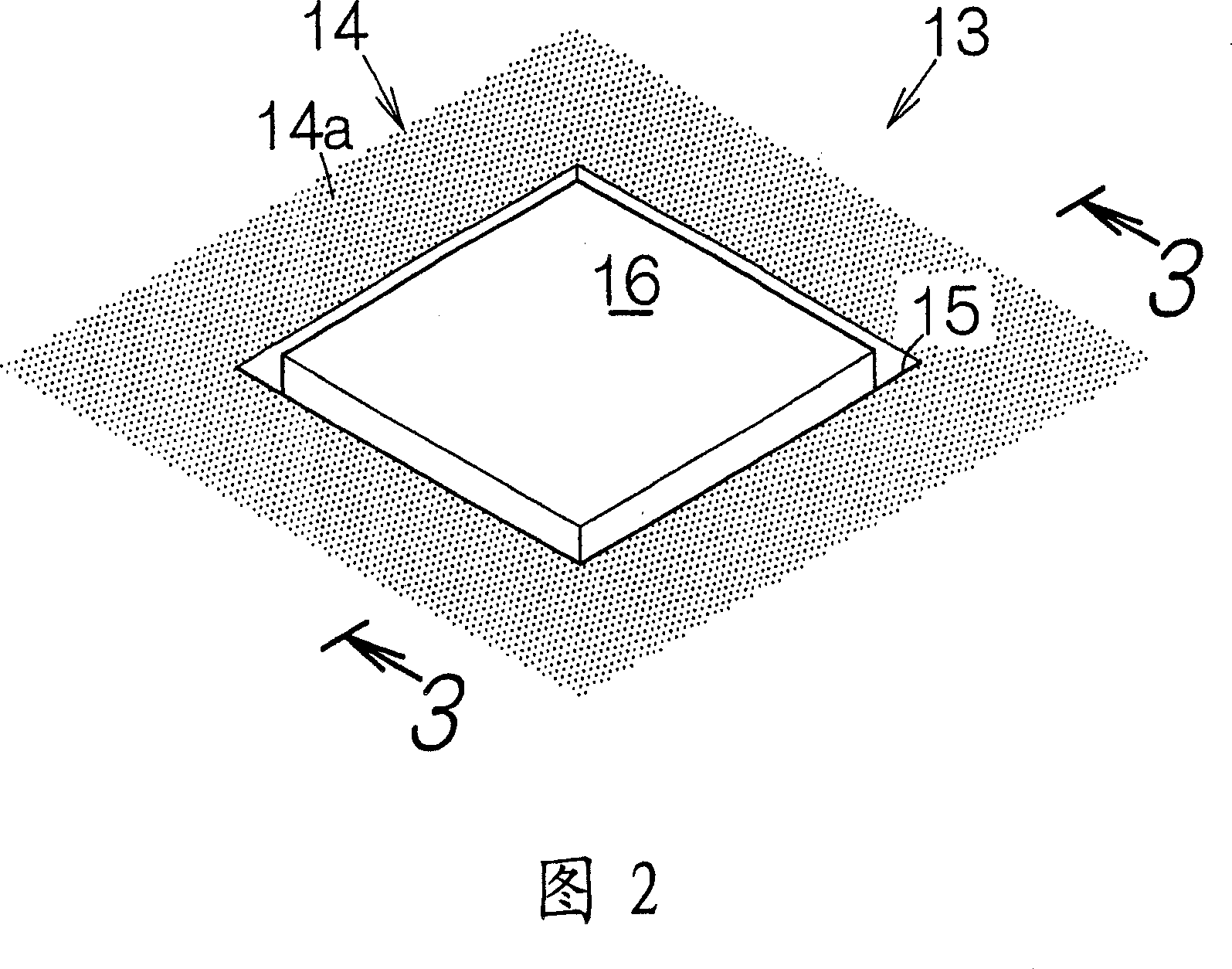
[0030] As shown in FIG. 2 , the motherboard unit 13 includes a printed wiring board 14 . The printed wiring board 14 includes a substrate 14a. A recess 15 is formed in the front surface of the substrate 14a. The depression 15 forms, for example, a cuboid-shaped space. Electronic components or large scale integration (LSI) chips 16 are accommodated in the recess 15 . The LSI chip 16 is a so-called Insert Mounted Device (IMD).

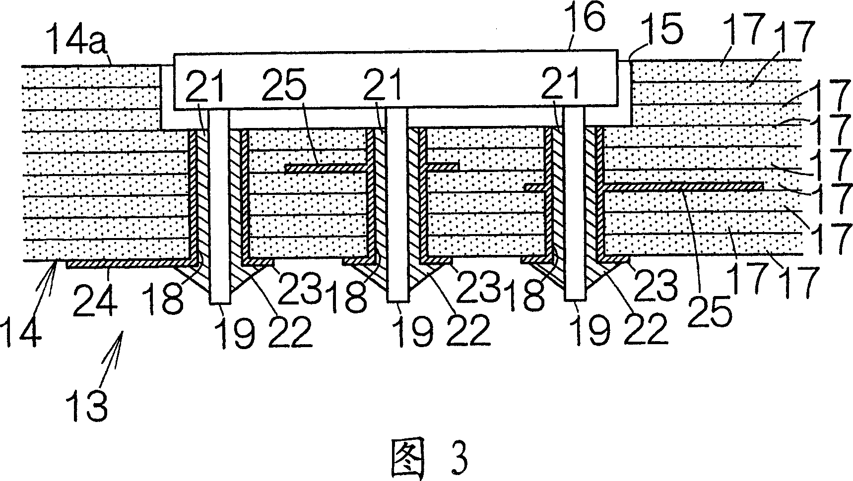
[0031] As shown in FIG. 3 , the substrate 14 a has a layered structure including a plurality of insulating layers 17 . The insulating layer 17 can be made of a resin material, for example. For example, a thro...


PUM


Abstract

The present invention opens a printed circuit board unit. A sunken hole is formed in the first surface of the printed circuit board. The through hole runs through the printed circuit board from the sunken bottom surface to the second surface of the printed circuit board. The second surface is the opposite surface of the first surface. The terminal of the electron assembly block is accommodated in the through hole. The bottom of the terminal protrudes from the second surface of the printed circuit board. The through hole is filled with solder. It makes the bottom of the terminal protrude from the second surface of the printed circuit board even if the terminal is shorter than the original thickness of the printed circuit board. It need not change the length of the terminal.

Description

technical field [0001] The invention relates to a printed circuit board unit. Specifically, the printed circuit board unit includes: a printed wiring board; a through hole penetrating the printed wiring board from a first surface of the printed wiring board to a second surface of the printed wiring board, the second surface being the first surface an opposite surface; an electronic component located on the first surface or the second surface of the printed wiring board; and a terminal mounted on the electronic component, the terminal passing through the through hole. Background technique [0002] For example, as disclosed in Japanese Patent Application Publication No. 1-238091, electronic components are mounted on the back side of a printed wiring board. Terminals or leads of the electronic components are received respectively in through holes defined in the printed wiring board. The ends of the wires are located in recesses formed on the front surface of the printed wirin...

Claims


Application Information

Patent Timeline
Patent Type & Authority Applications(China)
IPC IPC(8): H05K1/18
CPCH05K2201/09472H05K3/3447H05K1/116H05K3/429H05K2203/0228H05K1/183H05K2201/09036H05K2201/10704
Inventor 松井亚纪子
Owner FUJITSU LTD
Why Eureka
Try Eureka