Liquid crystal display panel data signal distortion compensating process and circuit

A technology for liquid crystal display panels and data signals, applied in static indicators, instruments, etc., can solve the problems of uneven brightness at the top and bottom of the display panel and the center, unable to effectively improve uneven brightness, and increase costs.

Active Publication Date: 2008-06-04
INNOLUX CORP
View PDF5 Cites 26 Cited by
  • Summary
  • Abstract
  • Description
  • Claims
  • Application Information

AI Technical Summary

Problems solved by technology

However, a double drive assembly is required, which necessitates a considerable additional cost
Furthermore, when the size of the liquid crystal display panel increases to a certain extent, the current improved method of using double-sided driving, because the unilateral resistance-capacitance effect b

Method used


Image

  • Liquid crystal display panel data signal distortion compensating process and circuit
  • Liquid crystal display panel data signal distortion compensating process and circuit
  • Liquid crystal display panel data signal distortion compensating process and circuit

Examples


Embodiment Construction

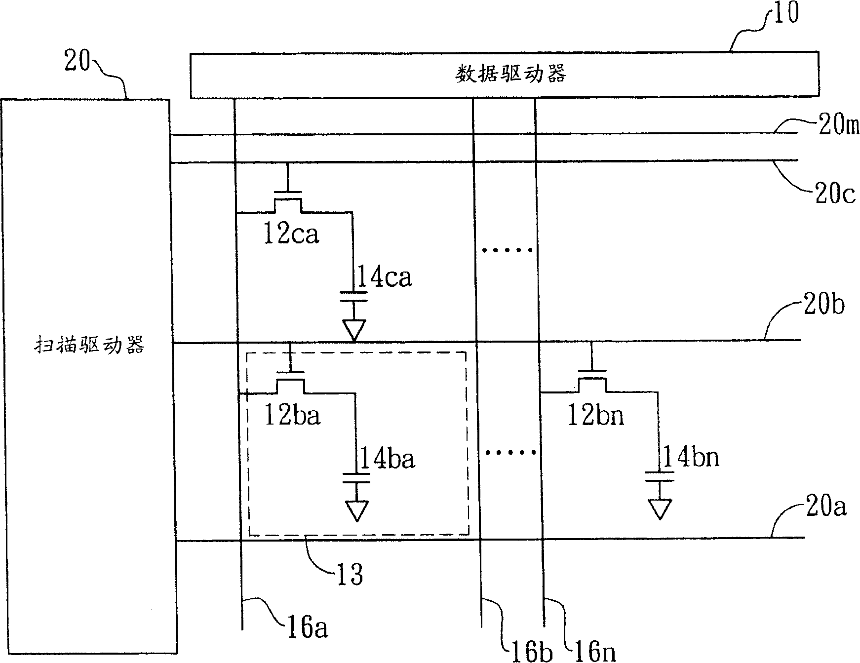
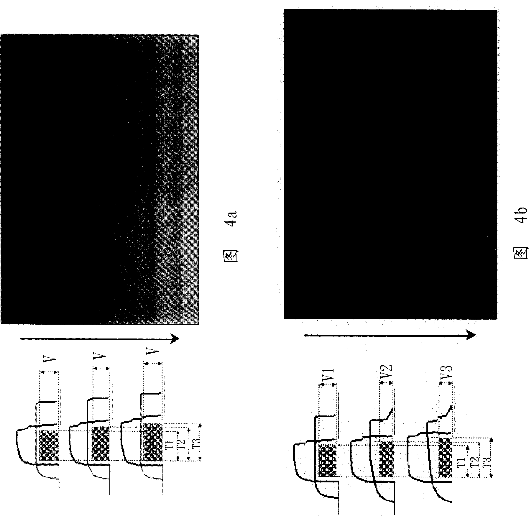
[0046] see figure 1 4a, it provides scanning signals with different turn-on time widths T1, T2, T3, . As shown in FIG. 4a, the signal waveform of the data signal of the ideal data line will not be distorted, and the scanning lines 20a, 20b, ... and 20m provide scanning lines with different turn-on time widths T1, T2, T3 ..., etc. Scanning the signal will result in different brightness changes. For example, when the on-time widths T1 , T2 , T3 . . . increase linearly from top to bottom, the vertical brightness of the liquid crystal display panel will show a linear change from top to bottom. Taking the transistors 12ba, 12ca, . Distortion, so that the total charge of the capacitors of the display units shows a linear change from top to bottom.

[0047]Please refer to FIG. 4 b , which is a schematic diagram of brightness compensation of a liquid crystal display panel according to a preferred embodiment of the present invention. Utilizing the characteristics shown in FIG. 4a a...


PUM


Abstract

The present invention relates to a data signal distortion compensation method and circuit for liquid crystal display panels, which is a method and a circuit that utilize adjusting the linear increase of the opening time width of scanning signals. As the total electric charge amount of the capacitance supplied to one row of display units can be the same, the reflected brightness can be the same as well. Therefore, the present invention can obviously improve the uneven brightness phenomenon caused by the on-line resistance-capacitance effect of data, so as to improve the phenomenon that liquid crystal display panels are uneven in brightness.

Description

technical field [0001] The invention provides a method and circuit for compensating data signal distortion of a liquid crystal display panel, especially a method and circuit for adjusting the opening time width of a scanning signal, so as to improve the phenomenon of uneven brightness of the liquid crystal display panel. Background technique [0002] Please refer to figure 1 , which is a schematic diagram of a conventional liquid crystal display panel. The liquid crystal display panel includes: a data driver 10 , a scan driver 20 , a plurality of display units, a plurality of scan lines and a plurality of data lines. Wherein, each set of interleaved data lines and scan lines can be used to control a display unit. For example: the data line 16a and the scan line 20b can be used to control the display unit 13, wherein the display unit 13 includes a transistor 12ba and a capacitor 14ba, and the gate and drain of the transistor 12ba are electrically connected to the scan line ...

Claims


Application Information

Patent Timeline
IPC IPC(8): G02F1/133G09G3/36
Inventor 杨鹦文黄永历
Owner INNOLUX CORP
Why Eureka
Try Eureka