
Pixel circuit, display device and driving method

A pixel circuit and drive circuit technology, which is applied to the pixel circuit of organic light-emitting diodes, display devices and drive fields, can solve problems such as uneven brightness, achieve the effects of increasing life, increasing aperture ratio, and improving uneven brightness

Active Publication Date: 2015-12-16
INNOCOM TECH (SHENZHEN) CO LTD +1
View PDF5 Cites 0 Cited by
  • Summary
  • Abstract
  • Description
  • Claims
  • Application Information

AI Technical Summary

Problems solved by technology

[0009] In view of the above problems, the object of the present invention is to provide a pixel circuit, a display device and a driving method that can not only improve the brightness unevenness caused by the variation of the element characteristics of the driving transistor of the display device, but also improve the aperture ratio of the display device.

Method used


Image

  • Pixel circuit, display device and driving method
  • Pixel circuit, display device and driving method
  • Pixel circuit, display device and driving method

Examples


no. 1 example

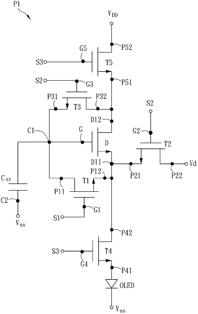
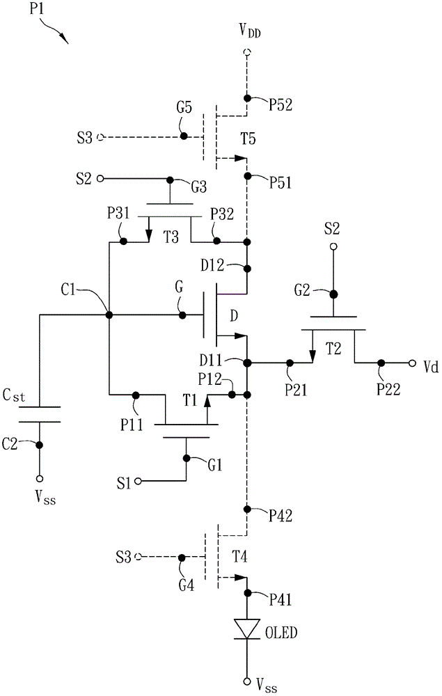
[0056] Please refer to Figure 2A As shown, it is a schematic circuit diagram of a pixel circuit P1 according to the first embodiment of the present invention.

[0057] The pixel circuit P1 of the present invention includes an energy storage element Cst, a driving transistor D, a first transistor T1 and a second transistor T2. In addition, the pixel circuit P1 further includes a third transistor T3, a fourth transistor T4, a fifth transistor T5 and an organic light emitting diode OLED.

[0058] The gate G of the driving transistor D is electrically connected to the energy storage element Cst. Here, the energy storage element Cst is a capacitor, and the gate G of the driving transistor D is electrically connected to one terminal C1 of the energy storage element Cst, and the other terminal C2 of the energy storage element Cst is connected to a second voltage V SS Terminals are electrically connected (also electrically connected to a first voltage V DD end).

[0059] The firs...

no. 2 example

[0071] Please refer to Figure 3A As shown, it is a schematic circuit diagram of a pixel circuit P2 according to the second embodiment of the present invention.

[0072] The pixel circuit P2 includes an energy storage element Cst, a driving transistor D, a first transistor T1 and a second transistor T2. In addition, the pixel circuit P2 further includes a third transistor T3, a fourth transistor T4 and an organic light emitting diode OLED.

[0073] The gate G of the driving transistor D is electrically connected to the energy storage element Cst. Here, the energy storage element Cst is a capacitor, and the gate G of the driving transistor D is electrically connected to one terminal C1 of the energy storage element Cst, and the other terminal C2 of the energy storage element Cst is connected to a DC bias ( positive or negative) to connect.

[0074] The first terminal P11 of the first transistor T1 is electrically connected to the terminal C1 of the energy storage element Cst...

no. 3 example

[0087] Please refer to Figure 4A As shown, it is a schematic circuit diagram of a pixel circuit P3 according to the third embodiment of the present invention.

[0088] The pixel circuit P3 includes an energy storage element Cst, a driving transistor D, a first transistor T1 and a second transistor T2. In addition, the pixel circuit P3 further includes a third transistor T3, a fourth transistor T4, a fifth transistor T5 and an organic light emitting diode OLED.

[0089] The gate G of the driving transistor D is electrically connected to the energy storage element Cst. Here, the energy storage element Cst is a capacitor, and the gate G of the driving transistor D is electrically connected to one terminal C1 of the energy storage element Cst, and the other terminal C2 of the energy storage element Cst is connected to a DC bias (positive and negative either) to connect.

[0090] The first terminal P11 of the first transistor T1 is electrically connected to the terminal C1 of t...


PUM


Abstract

The invention provides a pixel circuit which comprises an energy storage element, a driving transistor, a first transistor and a second transistor, wherein a grid electrode of the driving transistor is electrically connected with the energy storage element; a first end of the first transistor is electrically connected with grid electrodes of the energy storage element and the driving transistor respectively; a second end of the first transistor is electrically connected with a first end of the driving transistor; a first end of the second transistor is electrically connected with the first end of the driving transistor and the second end of the first transistor respectively; a second end of the second transistor is connected with data voltage or first voltage; in a first stage, grid electrodes of the first transistor and the second transistor receive a first signal and a second signal respectively; and the data voltage or the first voltage charges the energy storage element through the first transistor and the second transistor.

Description

technical field [0001] The present invention relates to a pixel circuit, a display device and a driving method, in particular to a pixel circuit, a display device and a driving method of an organic light emitting diode. Background technique [0002] Flat display apparatus (flat display apparatus) has been used in a variety of electronic products due to its advantages of low power consumption, low heat generation, light weight and non-radiation, and has gradually replaced traditional cathode ray tubes (cathoderay tubes). , CRT) display device. Flat panel display devices can generally be classified into passive matrix and active matrix according to their driving methods. The passive matrix display device is limited by the driving mode, so it has disadvantages such as short lifespan and incapable of large area. Although the active matrix display device has disadvantages such as higher cost and more complicated manufacturing process, it is suitable for full-color display with ...

Claims


Application Information

Patent Timeline
Patent Type & Authority Patents(China)
IPC IPC(8): G09G3/32G09G3/3233G09G3/3275
CPCG09G3/3233G09G2300/0819G09G2300/0842G09G2300/0861G09G2310/0251G09G2310/0262G09G2320/0233
Inventor 陈联祥郭拱辰曾名骏
Owner INNOCOM TECH (SHENZHEN) CO LTD
Learn More