Printed circuit boards coarse defect image detection method based on FPGA

A printed circuit board, image detection technology, applied in the direction of measuring electricity, measuring devices, measuring electrical variables, etc., can solve the problems of affecting detection efficiency, difficult to determine image differences, slow detection speed, etc., to improve work efficiency and reduce misjudgment and omission of judgment, to achieve the effect of accurate judgment

Inactive Publication Date: 2008-07-09
THE 45TH RES INST OF CETC
View PDF0 Cites 16 Cited by
  • Summary
  • Abstract
  • Description
  • Claims
  • Application Information

AI Technical Summary

Problems solved by technology

At present, the known detection methods are based on simple logical operations such as addition and subtraction of images. The analysis of the operation results is relatively simple, and it is difficult to determine the difference between images and the type of defect. Real-time processing, affecting detection efficiency

Method used


Image

  • Printed circuit boards coarse defect image detection method based on FPGA
  • Printed circuit boards coarse defect image detection method based on FPGA
  • Printed circuit boards coarse defect image detection method based on FPGA

Examples


Embodiment

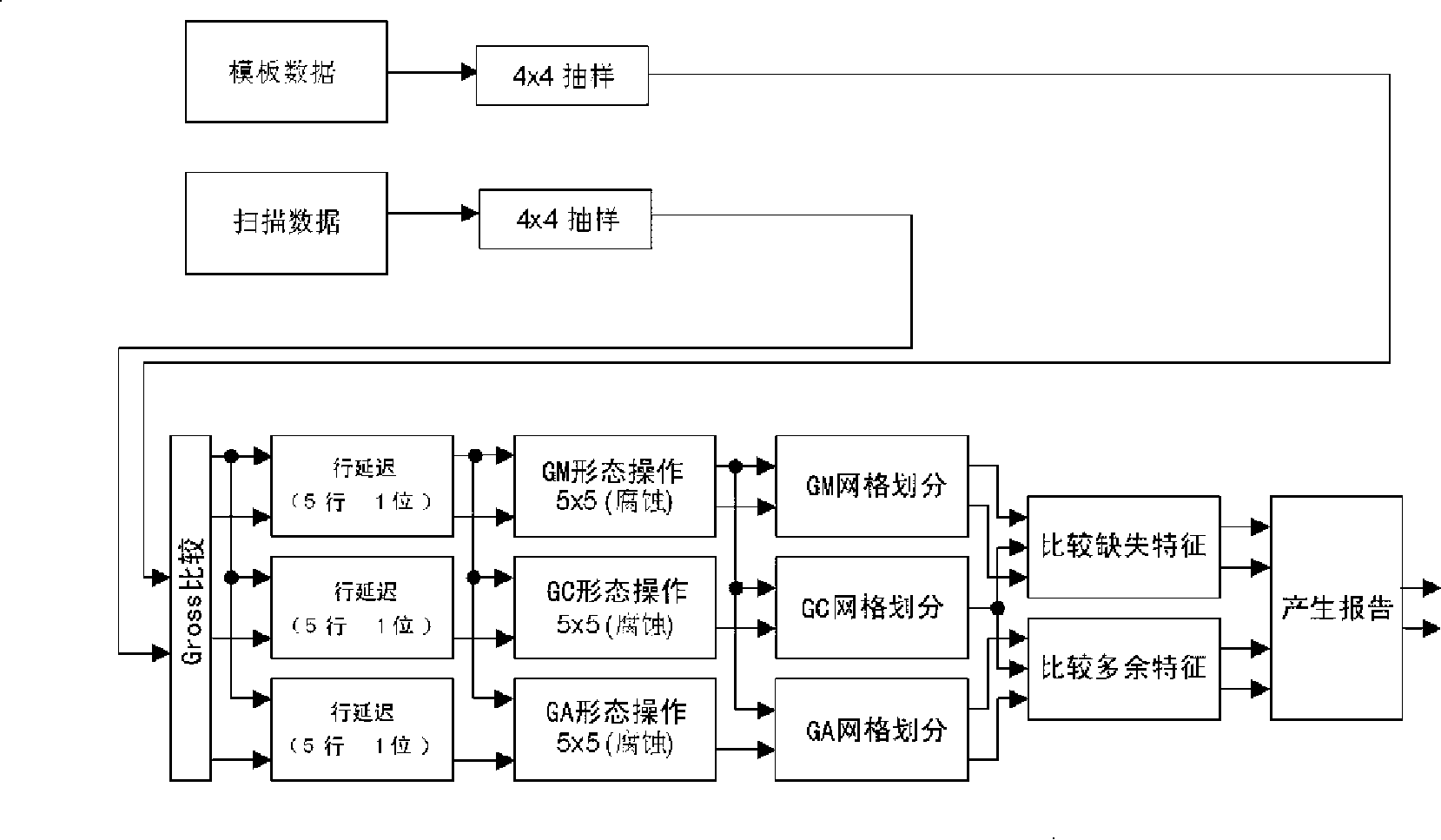
[0032] Embodiment: the present invention realizes algorithm description by using hardware description language VHDL, downloads to FPGA programmable gate array, adopts grid technology to carry out fast and effective analysis, processing to image, guarantees the fast and effective of algorithm and the accuracy of result.

[0033] Figure 6 The flow chart of the novel Gross algorithm based on FPGA provided by the present invention, the method may further comprise the steps:

[0034] Step 1: If figure 1 As shown, in the comparison module, input the data stream and parameters, input the preprocessed scanned image data and the template image data with the same angle as the scanned image, and wait for processing.

[0035] Step 2: If figure 2 As shown, the scanning data and the template data are respectively subjected to a 4×4 sampling operation, so the algorithm mainly detects large defects, and the subtle features can be ignored, so the image is sampled to reduce the amount of da...


PUM


Abstract

A method for detecting crude defect image of a printed circuit board based on FPGA comprises the following steps of: subjecting preprocessed template image data and the image data of the scanned printed circuit board to be detected to information extraction at the same proportion by using a field programmable gate array collection card; comparing the two image data after information extraction to obtain the difference, subjecting the difference image data and the template image data to binary morphologic operation corrosion, dividing grids, and removing fine characteristics of image data and keeping the larger characteristics; counting foreground pixels in each grid and respectively outputting data streams larger than, equal to and small than the template image data; and determining the desired characteristics and coordinates according to the output result, reducing the original coordinates of the large characteristics and determining large defect characteristics and coordinates of the printed circuit board. The invention can rapidly detect large defects of the printed circuit board in real time.

Description

(1) Technical field [0001] The invention relates to an optical automatic detection method of a printed circuit board. (2) Background technology [0002] Automatic optical inspection equipment and other machine vision equipment need to quickly detect defects caused by the printed circuit board production process. At present, the known detection methods are based on simple logical operations such as addition and subtraction of images. The analysis of the operation results is relatively simple, and it is difficult to determine the difference between images and the type of defect. Real-time processing affects detection efficiency. (3) Contents of the invention [0003] The purpose of the present invention is to provide an FPGA-based method for image detection of gross defects in printed circuit boards, to solve the technical problem of quickly detecting large defects in printed circuit boards in real time. [0004] To achieve the above object, the present invention adopts th...

Claims


Application Information

Patent Timeline
Patent Type & Authority Applications(China)
IPC IPC(8): G01N21/956G01R31/00
Inventor 姚立新付纯鹤张云连军莉邴守东魏祥英
Owner THE 45TH RES INST OF CETC
Why Eureka
Try Eureka