Semiconductor fabrication process formula management process

A technology of process formula and manufacturing process, which is applied in semiconductor/solid-state device manufacturing, electrical program control, program control in sequence/logic controller, etc., and can solve the problem that the process formulas in the two places are not synchronized, and there is no unified strategy and storage space Waste and other issues, to achieve the effect of reducing storage space requirements, improving efficiency, and solving synchronization problems

Inactive Publication Date: 2008-07-09
BEIJING NAURA MICROELECTRONICS EQUIP CO LTD
View PDF0 Cites 11 Cited by
  • Summary
  • Abstract
  • Description
  • Claims
  • Application Information

AI Technical Summary

Problems solved by technology

In the current implementation, both systems have independent process recipe storage locally, and the interaction between the two systems only focuses on the transfer of process recipes, and there is no unified strategy on the whole
This may cause problems such as waste of storage space, out-of-synchronization of process formulas in the two places, and complicated management.

Method used


Image

  • Semiconductor fabrication process formula management process
  • Semiconductor fabrication process formula management process

Examples


Embodiment Construction

[0051] The following examples are used to illustrate the present invention, but are not intended to limit the scope of the present invention.

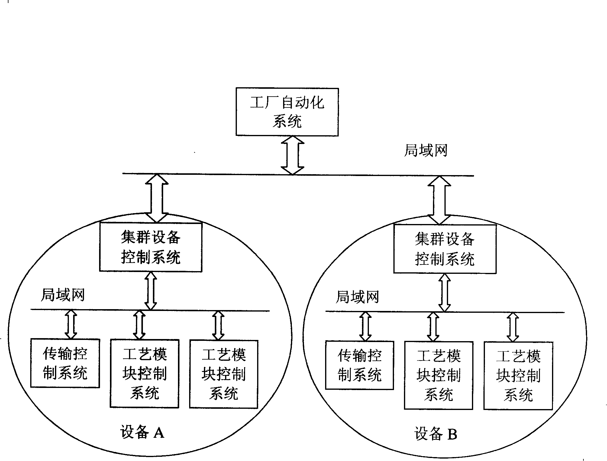
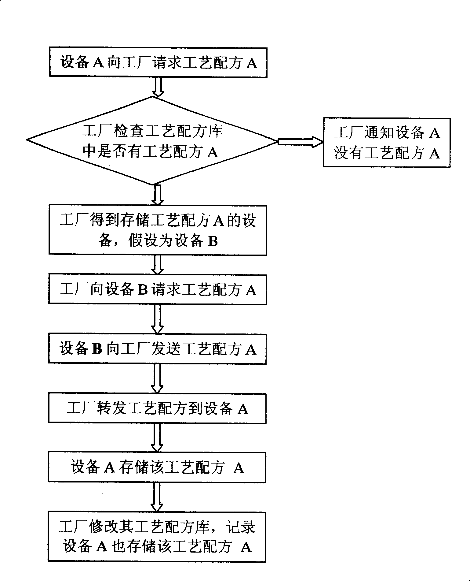
[0052] Currently there is a factory automation system (FA) and two devices (DA and DB respectively). Equipment A contains process recipes: RA1 (name), V1 (version number); RA2 (name), V1 (version number). Equipment B contains process recipes: RB1 (name), V1 (version number); RB2 (name), V1 (version number).

[0053] Initially, there is no connection between FA and DA, DB, and there is no record in its process recipe library.

[0054] After the connection between FA and DA is established, according to strategy 1, the process recipe library of FA will change, and it will record all the process recipes in device A, as shown in Table 1. Then FA establishes a connection with DB, and the contents of the final FA process formula library are shown in Table 2. During the above process, the process recipes stored in DA and DB have not been ch...


PUM


Abstract

The invention relates to the automation technical field of a semiconductor factory, in particular to a management method for semiconductor manufacturing process formulation. On the basis of dividing specific functional roles between a factory automation system and a device, the management method for the semiconductor manufacturing process formulation provided by the invention realizes the management on the process formulation in accordance with a plurality of strategies between the system and the device such as connection, disconnection and management. Through specifically dividing roles between the factory automation system and the device, two systems manage the process formulation coordinately, thereby decreasing the complexity of management and improving the efficiency of management.

Description

technical field [0001] The invention relates to the technical field of semiconductor factory automation, in particular to a method for managing recipes of semiconductor manufacturing processes. Background technique [0002] Semiconductor manufacturing is a high-tech industry, but also a high-investment industry. In order to achieve its operational goals and improve productivity, semiconductor manufacturing plants are increasingly automating their production management activities, among which the automation of semiconductor manufacturing equipment management is particularly important. figure 1 It is a software architecture diagram for realizing equipment management automation. [0003] As shown, semiconductor manufacturing facilities are typically clustered facilities. The definition of cluster equipment in the semiconductor standard is: an integrated manufacturing system that is physically connected together and can be used to process different process modules and transpor...

Claims


Application Information

Patent Timeline
Patent Type & Authority Applications(China)
IPC IPC(8): G05B19/04H01L21/00
Inventor 菅彦彬
Owner BEIJING NAURA MICROELECTRONICS EQUIP CO LTD
Why Eureka
Try Eureka