Method for accomplishing negative impulse annealing by data writing, its device and driver circuit

A data writing and negative pulse technology, which is applied in lighting devices, electric light sources, electrical components, etc., can solve the problems of failing to shorten the MPRT value of display devices, blurred image boundaries, and blurred dynamic pictures, so as to shorten the MPRT value and maintain Uniformity, yield improvement effect

Inactive Publication Date: 2008-08-06
上海广电光电子有限公司
View PDF0 Cites 17 Cited by
  • Summary
  • Abstract
  • Description
  • Claims
  • Application Information

AI Technical Summary

Problems solved by technology

This display technology has the disadvantage of a long Motion Picture Response Time (MPRT for short). As a result, when displaying a high-speed motion picture, the user will observe that the image boundary will appear blurred.
When the existing technology improves the life and uniformity of AMOLED devices, it cannot shorten the MPRT value of the display device, that is, it cannot solve the problem of blurred dynamic images.

Method used


Image

  • Method for accomplishing negative impulse annealing by data writing, its device and driver circuit
  • Method for accomplishing negative impulse annealing by data writing, its device and driver circuit
  • Method for accomplishing negative impulse annealing by data writing, its device and driver circuit

Examples


Embodiment Construction

[0062] The present invention will be further described below in conjunction with the accompanying drawings and embodiments.

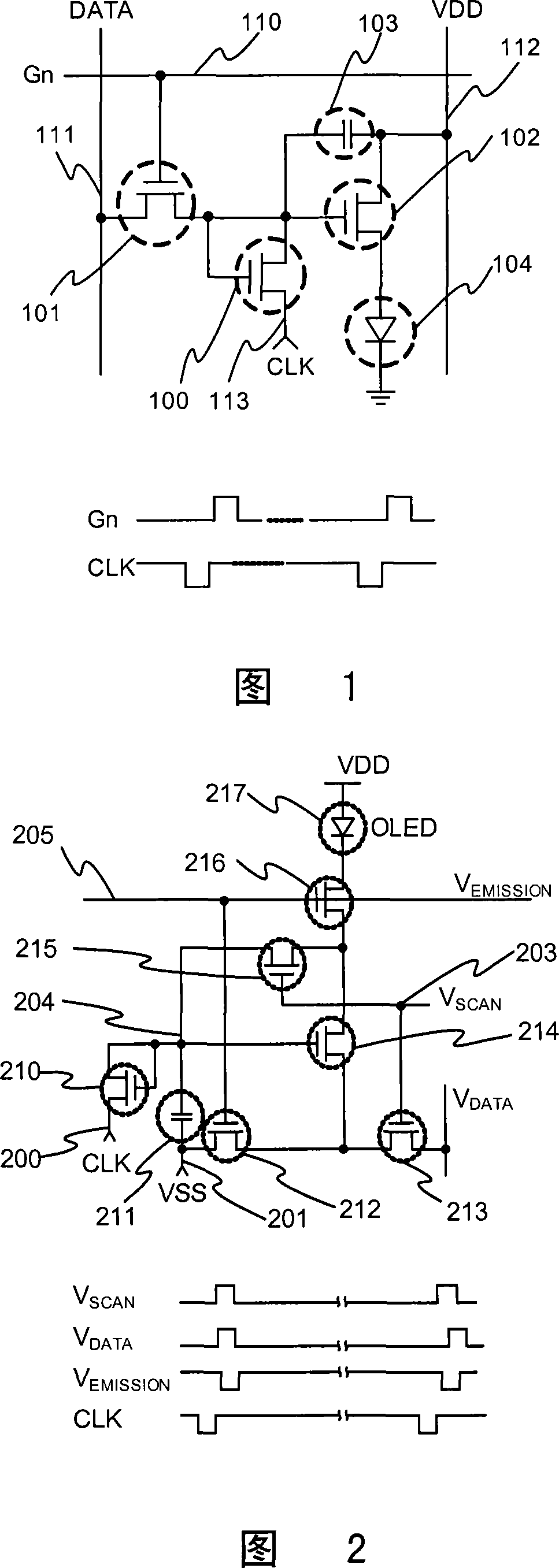
[0063] According to a specific implementation manner of the present invention, in a frame display period, firstly, in the first scan period, bias voltage data including display information is written to all pixels row by row. Then in the second scanning period, negative pulse voltage bias data including annealing pulse information is written to all pixels row by row.

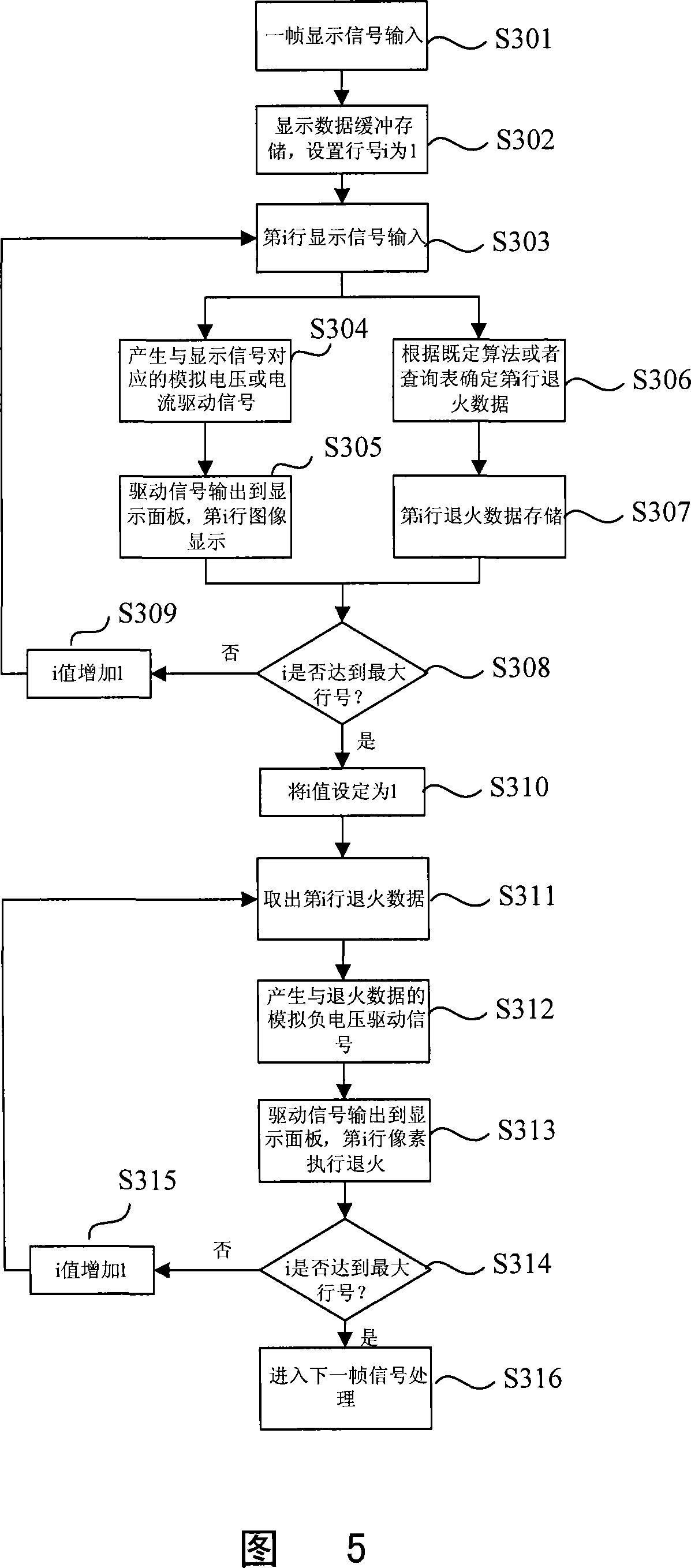
[0064] Referring to FIG. 3 , after a frame of display data is completely written, the image is displayed normally, as shown by 301 in FIG. 3 . In the following scanning period, the annealing voltage bias data is written row by row in a row scanning manner. When the writing is not completed, that is, in the middle of the scanning period when the annealing voltage bias data is written, some rows of pixels are written with annealing bias voltage data, and the OLED does not emit light; some ...


PUM


Abstract

The present invention discloses a method and a device for realizing negative impulse anneal by data writing, and a driving circuit thereof. The characteristic of a TFT in an active matrix driving OLED display device for driving OLED device is prevented from drifting, the service life of the device is prolonged. The technical proposal is that: within each frame display period, the method of the present invention comprises writing display data line by line for all pixels in a first scan period; writing anneal data line by line for all pixels in a second scan period. Or the method, in each frame display period, comprises writing the first part of the display data or the first part of the anneal data line by line for all pixels in the first scan period; writing the second part of the display data or the second part of the anneal data line by line for all pixels in the second scan period; wherein the display data is written into each pixel in one of the two scan periods of one frame display period, and the anneal data is written in the other scan period. The invention is applied in the liquid crystal display device field.

Description

technical field [0001] The present invention relates to a negative pulse annealing method, device and driving circuit for realizing black picture insertion, and in particular to a method, device and a negative pulse annealing method for implementing negative pulse annealing in a data writing mode applied in an active matrix organic light-emitting display. Drive circuit. Background technique [0002] An organic light emitting display device (OLED) is an active light emitting device. Compared with the current mainstream flat-panel display technology Thin Film Transistor Liquid Crystal Display (TFT-LCD), OLED has the advantages of high contrast, wide viewing angle, low power consumption, and thinner volume. It is one of the most concerned technologies in flat-panel display technology. [0003] OLEDs can be driven with either a passive matrix (PM) or an active matrix (AM). Compared with the PM driver, the AM driver has the advantages of larger displayed information capacity, l...

Claims


Application Information

Patent Timeline
Patent Type & Authority Applications(China)
IPC IPC(8): G09G3/32H05B33/08G09G3/3258H05B44/00
CPCY02B20/343Y02B20/346Y02B20/30
Inventor 李俊峰张晓建
Owner 上海广电光电子有限公司
Why Eureka
Try Eureka