Actively driven organic light emitting display

A light-emitting display device, source-driven technology, applied in static indicators, instruments, etc., can solve the problems of increasing the complexity of the system driving circuit, increasing the complexity of the system driving circuit, and the possibility of pixel failure, so as to reduce the design difficulty and implementation. cost, improving pixel area utilization, and suppressing characteristic drift

Active Publication Date: 2009-02-04
NANJING CEC PANDA LCD TECH
View PDF0 Cites 3 Cited by
  • Summary
  • Abstract
  • Description
  • Claims
  • Application Information

AI Technical Summary

Problems solved by technology

First of all, the circuit needs to introduce a negative voltage pulse signal for each pixel, so each row of pixels needs to add an additional signal wire, which reduces the pixel aperture ratio
Second, an external system drive circuit is required to provide a negative pulse generation circuit that cooperates with the scan drive signal, which increases the complexity of the system drive circuit
First, this design requires a top-emitting OLED device structure, and OLED fabrication is difficult to implement; second, compared with the basic AMOLED pixel, this circuit introduces multiple additional control signals, the wiring is complicated, and the complexity of the system driving circuit is greatly increased. ; Third, the number of devices in the pixel circuit is large, and the possibility of pixel failure in the process increases, which will lead to a decrease in product yield

Method used


Image

  • Actively driven organic light emitting display
  • Actively driven organic light emitting display
  • Actively driven organic light emitting display

Examples


Embodiment Construction

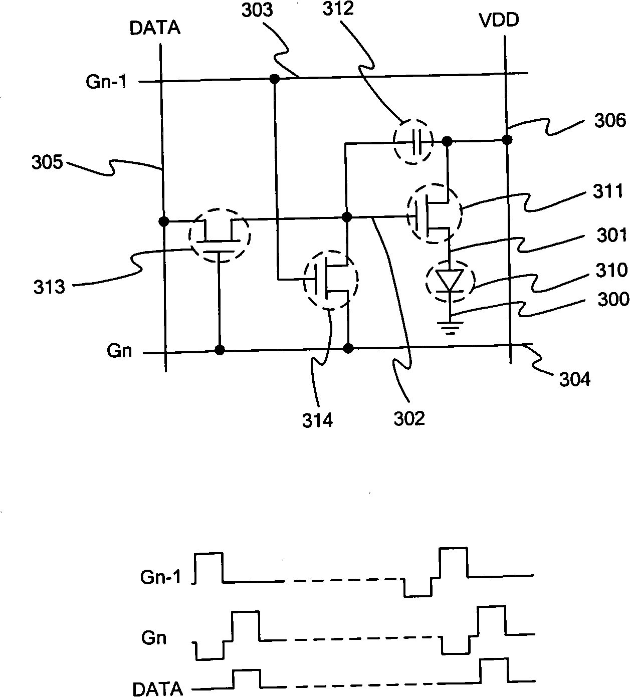
[0046] In the present invention, through the design of the pixel circuit, the signal of the negative bias voltage is realized through the connection inside the pixel or between the pixel and adjacent pixels, avoiding additional signal wiring for generating the negative bias signal. A negatively biased bias voltage signal is generated through the gate line.

[0047] refer to image 3 , which is a pixel equivalent circuit and its signal waveform diagram of the embodiment of the present invention.

[0048] As shown in the figure, the present invention includes three transistors: a first TFT 311 , a second TFT 313 , a third TFT 314 , a first capacitor 312 , and a first OLED 310 . TFT 311 is controlled by the voltage signal on its gate electrode, namely node 302, to supply power to OLED TFT 310; TFT 313 is controlled by the signal on gate scanning line 304 to write the signal on data line 305 into node 302; TFT 314 accepts The control of the gate scanning line 303 provides a disc...


PUM


Abstract

The invention provides a pixel circuit which improves the service life of the active matrix organic light-emitting device and comprises a first TFT, a second TFT, a third TFT, a first capacitor, a first organic light-emitting diode (OLED), a first gate scanning signal line, a second gate scanning signal line, a data signal line and a power signal line; the second gate scanning line of the current pixel line is composed of the first gate scanning line which is adjacent to the pixel line; the first TFT controls the power supply of the first OLED; the second TFT controls the time when the signal of the data line is written into the gate electrode node of the first TFT; the third TFT provides the discharge pathway which is from the first TFT gate electrode node to the first gate scanning signal line; the capacitor is used for storing charges and maintaining the voltage of the corresponding node; the organic light-emitting diode (OLED 310) is used for executing the light-emitting operation.

Description

technical field [0001] The invention relates to an active-driven organic light-emitting display device, belonging to the technical field of light-emitting display devices. Background technique [0002] Organic light emitting devices (OLEDs) can be driven by passive matrix (PM) or active matrix (AM). Compared with the PM driver, the AM driver has the advantages of larger displayed information capacity, lower power consumption, longer device life, and higher picture contrast. The PM drive is suitable for low-cost, simple display devices. [0003] Currently, there are basically two types of devices for AM-driven OLED fabricated on glass substrates, namely amorphous silicon (a-Si) thin film transistor (TFT) and low temperature polysilicon (LTPS) TFT. [0004] TFT devices will drift in device characteristics when they work in a DC voltage bias state for a long time. If some measures are not taken to deal with this drift, the device with characteristic drift will reduce the cur...

Claims


Application Information

Patent Timeline
Patent Type & Authority Applications(China)
IPC IPC(8): G09G3/32G09G3/3233
Inventor 李俊峰
Owner NANJING CEC PANDA LCD TECH
Why Eureka
Try Eureka