Image sensors, its forming method and semiconductor device

An image sensing and semiconductor technology, applied in the field of image sensing devices and their formation, can solve problems such as poor color separation, reduced spatial resolution sensitivity, etc., achieve high efficiency and cost-effectiveness, reduce electron overflow phenomenon, and be easy to integrate Effect

Inactive Publication Date: 2008-09-10
TAIWAN SEMICON MFG CO LTD
View PDF0 Cites 2 Cited by
  • Summary
  • Abstract
  • Description
  • Claims
  • Application Information

AI Technical Summary

Problems solved by technology

This phenomenon reduces spatial resolution and sensitivity, and leads to poor color separation

Method used


Image

  • Image sensors, its forming method and semiconductor device
  • Image sensors, its forming method and semiconductor device
  • Image sensors, its forming method and semiconductor device

Examples


Embodiment Construction

[0032] The concepts of the present invention will be described below through examples, and each example is only for illustration purposes, and is not intended to limit the scope of the present invention. In the drawings or descriptions, similar or identical parts will be given similar or identical reference numerals. In the drawings, the shape or thickness of elements may be enlarged or reduced. Components not shown or described in the figures may be in forms known to those skilled in the art. In addition, when the described layer is on a substrate or another layer, the layer may be directly on the substrate or another layer, or there may be an intervening layer therebetween.

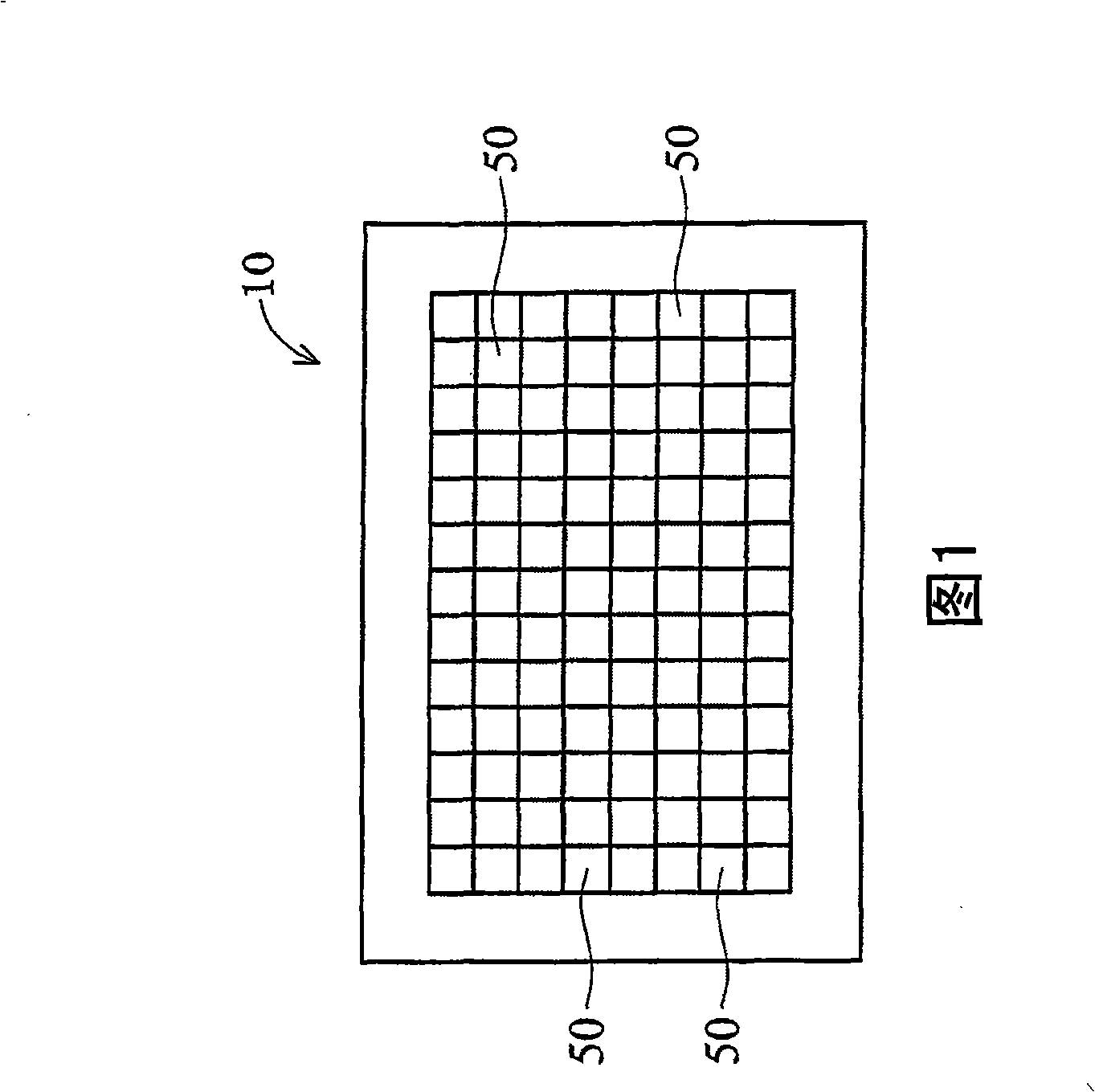
[0033] Please refer to FIG. 1 , which is a top view illustrating an image sensing device 10 according to an embodiment of the present invention. The image sensing device 10 includes pixels 50 arranged in a grid or an array, and the pixels 50 may also be referred to as image sensing elements. Addition...


PUM


Abstract

The present invention provides an image sensing device, the forming method and a semiconductor device thereof, wherein the image sensing device comprises the following components: a semiconductor substrate which has a first type of conductivity; a first material layer which has the first type of conductivity at the upper part of the semiconductor substrate; a second material layer which has a second type of conductivity at the upper part of the first material layer, wherein the second type of conductivity is different from the first type of conductivity; and a plurality of pixels existing in the second material layer. The device of the invention and the preparing method thereof can reduce the crosstalk disturbance and the electric spill phenomenon. Besides, the device provided by the invention and the preparing method thereof can easily confirmed with the prior semiconductor technological equipment and technique. The device provided by the invention and the preparing method thereof can avoid the ultimate of the technological equipment and the technique. Furthermore, the device provided by the invention and the preparing method thereof are suitable for the dimension of the pixel reducing continuously.

Description

technical field [0001] The present invention relates to a semiconductor device and its forming method, and in particular to an image sensing device and its forming method. Background technique [0002] In semiconductor technology, an image sensor can be used to sense light projected onto a semiconductor substrate. Complementary metal oxide semiconductor (CMOS) image sensors and charge-coupled device (CCD) sensors have been widely used in various fields, such as digital still cameras. These sensors utilize pixel arrays or image sensing elements, which may include photodiodes and MOS transistors, to receive light energy to convert the image into digital data. [0003] However, image sensing devices face problems of cross-talk and / or blooming. Light targeted to an image sensing element and electrical signals generated by the light may spread to adjacent image sensing elements. In some cases, high-intensity light creates excess electrons that overflow to other image-sensing e...

Claims


Application Information

Patent Timeline
Patent Type & Authority Applications(China)
IPC IPC(8): H01L27/146
CPCH01L27/14654
Inventor 洪志明杨敦年
Owner TAIWAN SEMICON MFG CO LTD
Why Eureka
Try Eureka