Flat panel display

A flat-panel display and substrate technology, applied in the direction of image/graphic display tubes, instruments, electric solid-state devices, etc., can solve problems such as uneven supply of voltage, non-maintenance of electrodes, uneven brightness of display devices, etc.

Inactive Publication Date: 2008-09-24
SAMSUNG SDI CO LTD
View PDF0 Cites 9 Cited by
  • Summary
  • Abstract
  • Description
  • Claims
  • Application Information

AI Technical Summary

Problems solved by technology

Therefore, the voltage value supplied to each electrode may not be maintained at a predetermined level
In addition, since a voltage of a predetermined level may not be uniformly supplied to the electron emission unit corresponding to each electrode, the amount of electrons emitted from each electron emission unit varies.
Therefore, the brightness of the display device may not be uniform for each pixel

Method used


Image

  • Flat panel display
  • Flat panel display
  • Flat panel display

Examples


Embodiment Construction

[0027] Reference will now be made in detail to embodiments of the invention, examples of which are illustrated in the accompanying drawings, like reference numerals referring to like elements throughout. The embodiments are described below in order to explain the present invention by referring to the figures.

[0028]The dimensions of layers and regions in the drawings are exaggerated for clarity. It will also be understood that when a layer or element is referred to as being "on" or "over" another layer or substrate, it can be directly on the other layer or substrate, or intervening layers may also be present. Further, it will also be understood that when a layer is referred to as being "under" or "under" another layer, it can be directly under, and one or more intervening layers may also be present.

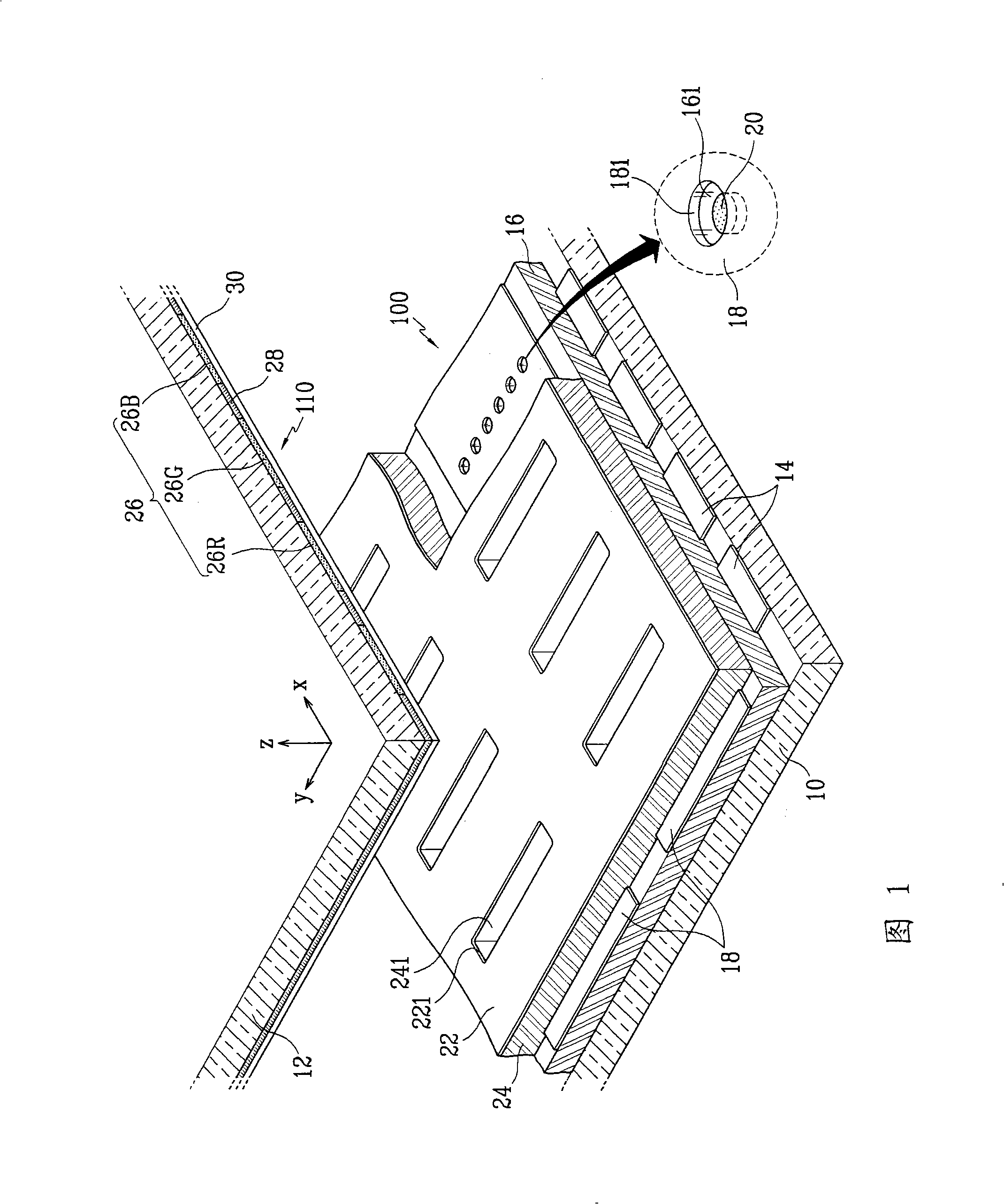
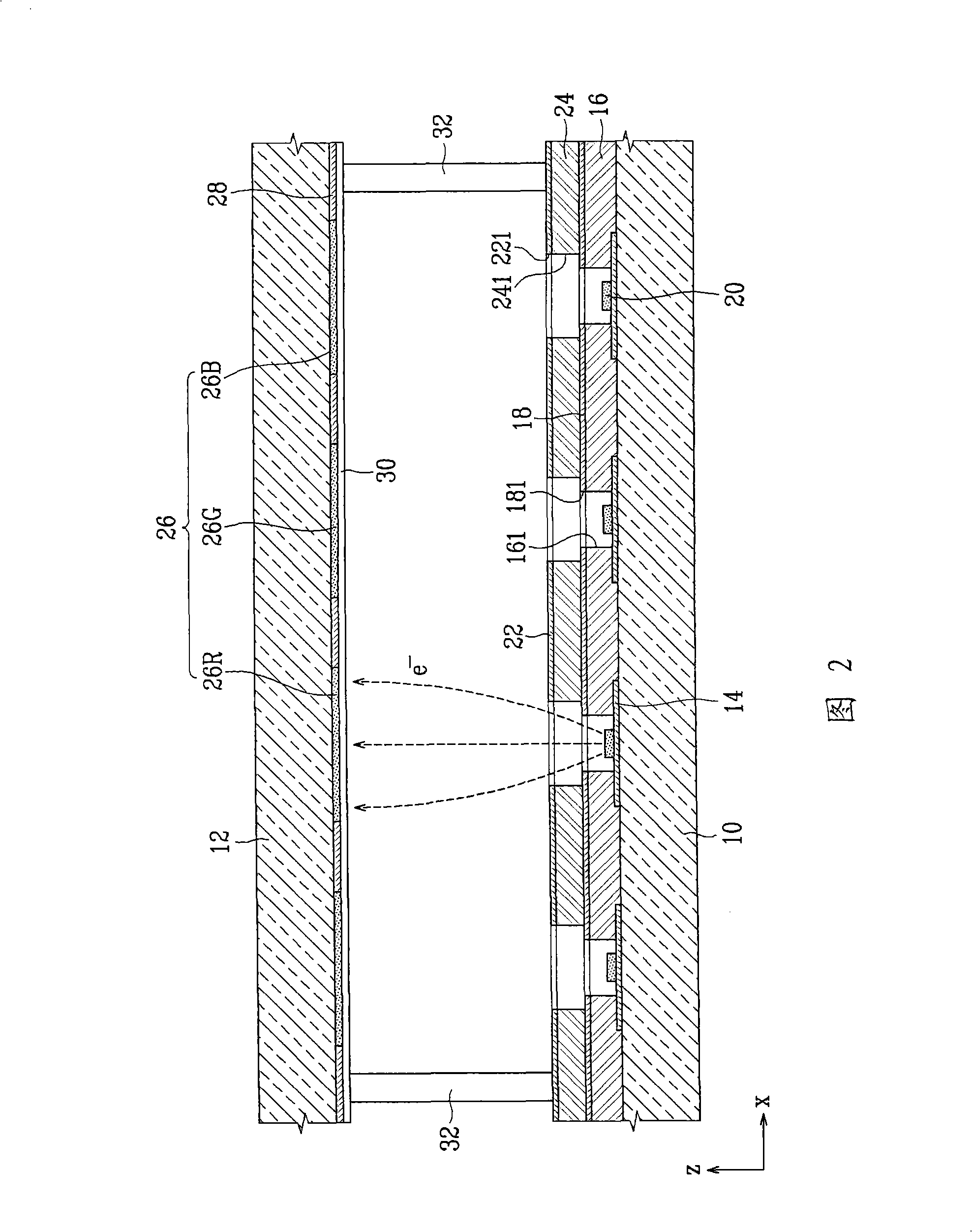
[0029] FIG. 1 is a partially exploded perspective view of a flat panel display according to an embodiment of the present invention. FIG. 2 is a cross-sectional view of the fl...


PUM


Abstract

A flat panel display to maintain resistance of lines at the same level to reduce a luminance difference between the lines includes a plurality of electrodes (14) and a plurality of lead lines (36) to respectively connect a plurality of pads (34) to the plurality of electrodes (14). The lead lines (36) are formed in a parallelogram shape in which resistivity and line thickness are the same for each lead line, and a length L and a line width W of each lead line are selected such that a value obtained by dividing the length L by the line width W satisfies the equation:; L 1 W 1 = L 2 W 2 = L 3 W 3 = | | = L n W n , where L1, L2, L3, ..., and Ln respectively refers to long side lengths, which are direct line distances between the electrode (14) and the pad (34), of the respective lead lines (36) formed in the parallelogram shape, and W1, W2, W3, . , and Wn respectively refers to widths, which are short side distances of the respective lead lines (36) formed in the parallelogram shape.

Description

technical field [0001] The present invention relates to flat panel displays. More particularly, the present invention relates to electrode patterns for flat panel displays. Background technique [0002] Generally, a flat panel display (FPD) includes a front substrate and a rear substrate combined to form a closed and sealed container having a predetermined inner space. A structure that emits light of a predetermined color from each pixel is provided in a sealed container so as to realize or display an image. [0003] There are various types of flat panel displays, including liquid crystal displays (LCDs), plasma display panels (PDPs), vacuum fluorescent displays, electron emission displays, and organic light emitting diode (OLED) displays. Since the flat panel display includes electrodes for driving the flat panel display, the electrodes are formed in a predetermined pattern on the front substrate or the rear substrate. Ends of the electrodes are connected to pads connect...

Claims


Application Information

Patent Timeline
Patent Type & Authority Applications(China)
IPC IPC(8): H01J5/46H01J29/90H01J29/02H01J17/18H01J31/12G02F1/1345H01L51/52G09F9/00
CPCH01J29/92H05K1/117H01L27/3276H01J31/127G02F1/1345H05K2201/09727H05K2201/0784H01J2329/92H05K2201/09236H10K59/131H01J1/30H05B33/26H01J29/02
Inventor 李炳坤
Owner SAMSUNG SDI CO LTD
Why Eureka
Try Eureka