Module and electronic device

An electronic device and intermediate position technology, applied in the field of electronics, can solve the problems of cumulative tolerance of the dimension chain and the difficulty of guaranteeing pin coplanarity, and achieve the effect of eliminating the cumulative dimensional error, reducing the layout space, and improving the coplanarity.

Active Publication Date: 2008-11-05
HUAWEI TECH CO LTD
View PDF0 Cites 8 Cited by
  • Summary
  • Abstract
  • Description
  • Claims
  • Application Information

AI Technical Summary

Problems solved by technology

In the process of realizing the present invention, the inventors found that there are at least the following problems in the prior art. In this implementation scheme, since different pin structures are used on both sides of the module substrate, and two pairs of positioning holes parallel to each other are used for positioning on the substrate. , there are shortcomings such as cumulative tolerances in the dimensional chain, and difficulty in ensuring the coplanarity of the pins.

Method used


Image

  • Module and electronic device
  • Module and electronic device
  • Module and electronic device

Examples


Embodiment Construction

[0035] In order to make the object, technical solution and advantages of the present invention clearer, the present invention will be further described in detail below with reference to the accompanying drawings and examples.

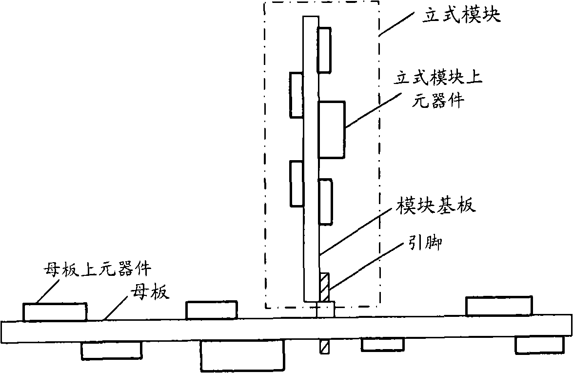
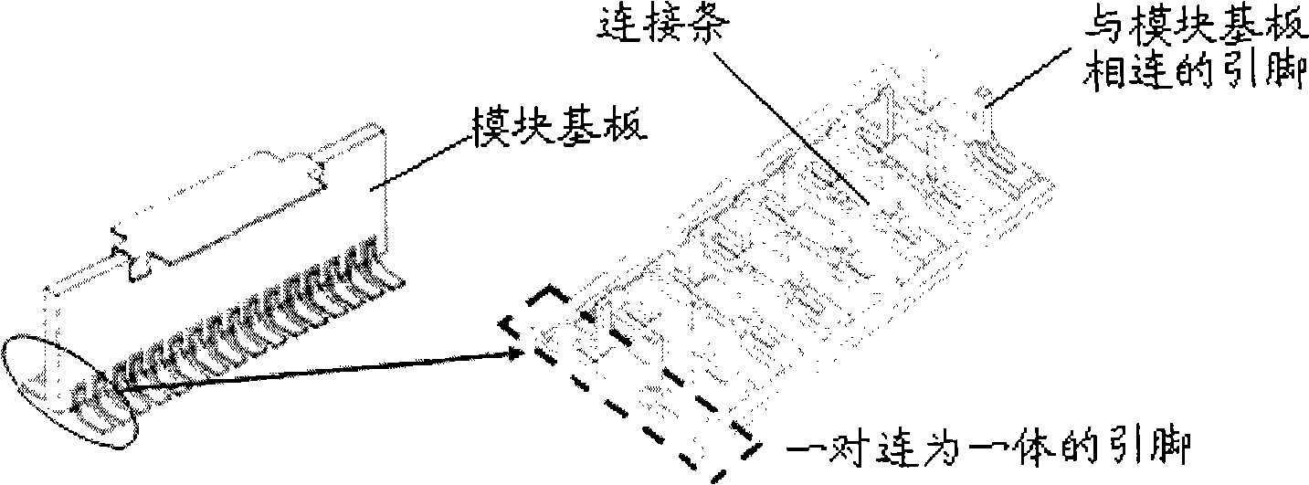
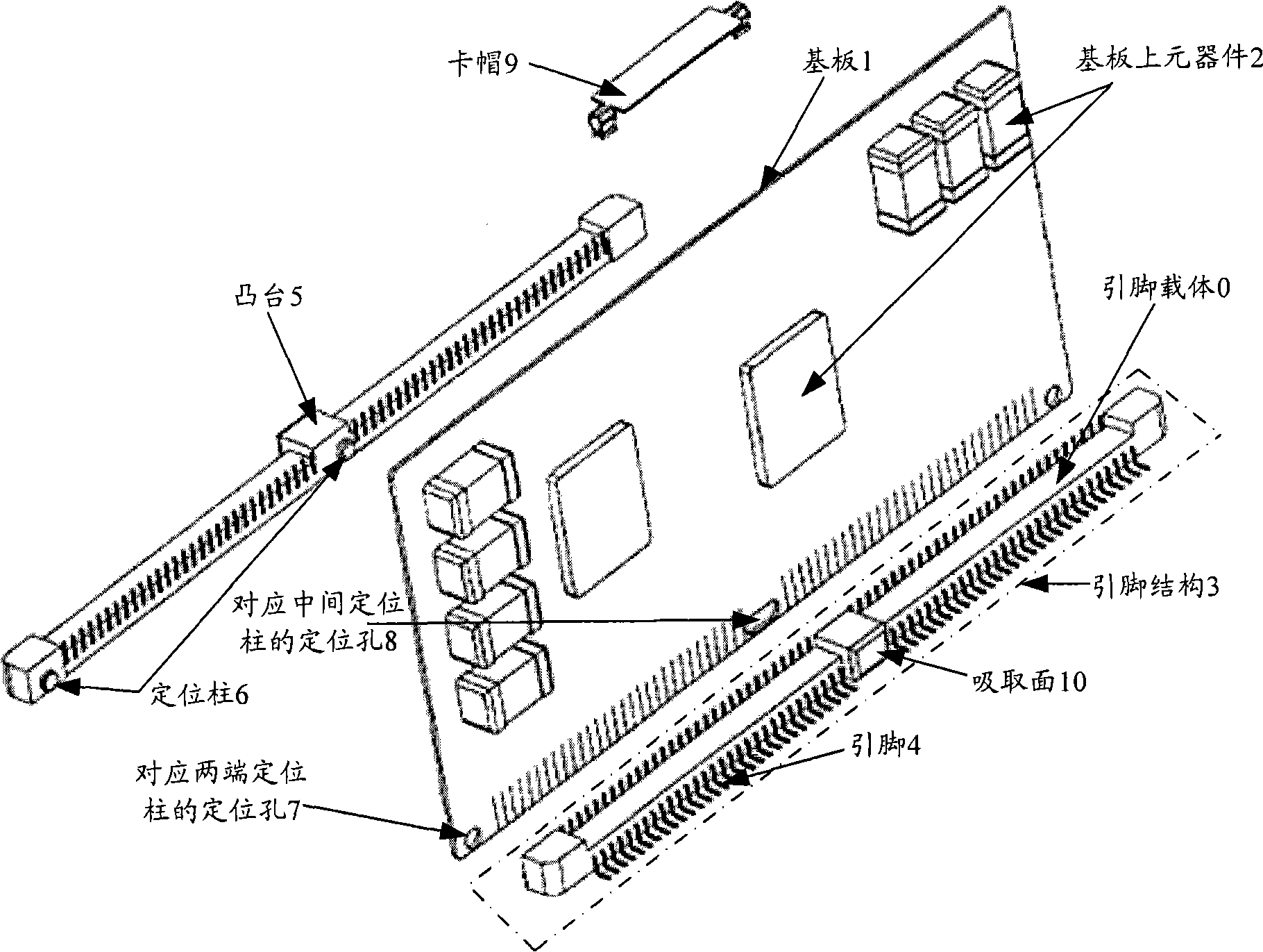
[0036] The module of the present invention mainly includes a substrate and a pin structure.

[0037] Wherein, the pin structure includes a pin and a pin carrier; the pins are independently mounted on the pin carrier; the pin structure is at least two, which are respectively arranged on both sides of the substrate for connecting the substrate and motherboard;

[0038] When the substrate is relatively long, two or more pin structures can be respectively arranged on the same side of the substrate to improve the stability of the connection between the substrate and the motherboard.

[0039] The pin carrier is provided with at least two positioning columns, and the substrate is provided with positioning holes corresponding to the positioning columns provide...


PUM


Abstract

The invention discloses a module including a base plate and two pin structure, wherein the pin structure comprises a pin and a pin carrier; each pin is independently sticked on the pin carrier; at least two pin structures are provided respectively arranged at the two sides of the base plate for connecting the base plate and the motherboard; at least two reference columns are arranged on the pin carrier. A positioning hole corresponding to the reference column arranged on the pin structure is arranged on the base plate, wherein the positioning hole on the base plate is on the same line; the reference column on the pin carrier is assembled with the base plate. The invention also discloses an electronic equipment including a module and a motherboard. The pins at the two sides of the base plate is independant each other for connecting different I / O ports, which advances the layout density, thereby reducing the layout space of the motherboard, increasing the whole layout density, meanwhile the positioning hole on the module base plate is on the same level, which effectively ensures the coplane degree of the vertical module pin.

Description

technical field [0001] The invention relates to the field of electronic technology, in particular to a vertical module and an electronic device. Background technique [0002] High-density miniaturization is the development trend of electronic products, and it is also a challenge that the electronic assembly process has been facing. Increasing the layout density of single boards has become one of the necessary conditions for the realization of high-density miniaturization of electronic products. [0003] Integrate part of the common circuits on the circuit board, especially the circuit units repeated many times on a motherboard, into the module, and then assemble it on the motherboard as a conventional device. This method not only makes full use of the three-dimensional space and reduces the occupied area, but also improves the assembly efficiency and quality while increasing the layout density, and reduces the production cost. [0004] Module (Module) is neither a special s...

Claims


Application Information

Patent Timeline
Patent Type & Authority Applications(China)
IPC IPC(8): H01L25/00H01L23/488
CPCH01R12/721H01R12/716H01R23/7068
Inventor 陈松柏
Owner HUAWEI TECH CO LTD
Why Eureka
Try Eureka