Organic LED and manufacture method thereof

A technology for light-emitting diodes and a manufacturing method, applied in the directions of organic semiconductor devices, semiconductor/solid-state device manufacturing, electrical components, etc., can solve problems such as poor hole injection effect, avoid separation phenomenon, improve hole injection effect, and improve adhesion. Sexually Inferior Effects

Active Publication Date: 2010-05-26
INNOCOM TECH (SHENZHEN) CO LTD +1
View PDF2 Cites 0 Cited by
  • Summary
  • Abstract
  • Description
  • Claims
  • Application Information

AI Technical Summary

Problems solved by technology

[0007] In order to solve the problem of poor hole injection effect of organic light emitting diodes in the prior art, it is necessary to provide an organic light emitting diode with better hole injection effect

Method used


Image

  • Organic LED and manufacture method thereof
  • Organic LED and manufacture method thereof
  • Organic LED and manufacture method thereof

Examples


Embodiment Construction

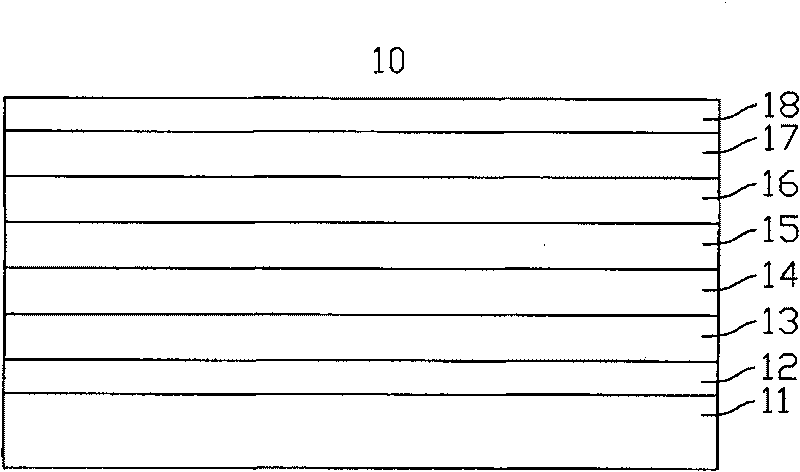
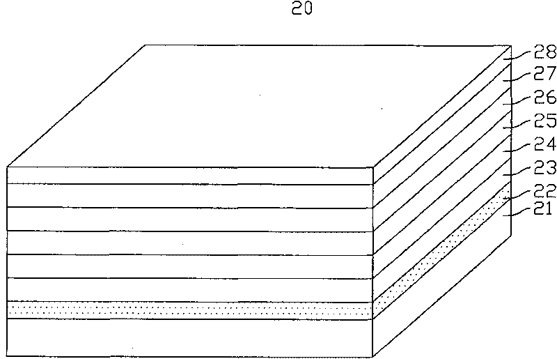
[0016] see figure 2 , is a three-dimensional schematic view of a preferred embodiment of the organic light emitting diode of the present invention. The OLED 20 includes a substrate 21, an anode 22 stacked on the substrate 21 from bottom to top, a hole injection layer (Hole Injection Layer, HIL) 23, a hole transport layer (Hole Transfer Layer, HTL) 24, an organic light-emitting layer 25, an electron transfer layer (Electron Transfer Layer, ETL) 26, an electron injection layer (Electron Injection Layer, EIL) 27 and a cathode 28, wherein the material of the hole injection layer is organic Material, the anode 22 is made of indium tin oxide (Indium Tin Oxide, ITO) or indium zinc oxide (Indium Zinc Oxide, IZO), and the anode 22 has fluorine ions that can enhance hydrophobicity.

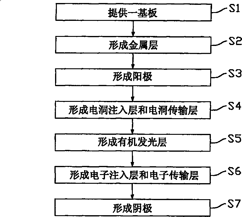
[0017] see image 3 ,yes figure 2 Flowchart of the OLED fabrication method shown. The organic light emitting diode manufacturing method includes the following steps: providing a substrate (S1); formin...


PUM


Abstract

The invention relates to an organic light emitting diode (LED) and a manufacturing method thereof. The organic LED comprises an insulation substrate, an anode, a hole implanted layer, a hole transferlayer and an organic emitting layer; the anode, the hole implanted layer, the hole transfer layer and the organic emitting layer are arranged on the insulation substrate in sequence; wherein, the anode is provided with fluorinion. The organic LED has better hole implanting effect.

Description

technical field [0001] The invention relates to an organic light emitting diode (Organic Light Emitting Diode, OLED) and a manufacturing method thereof. Background technique [0002] In recent years, organic light-emitting diodes have attracted the attention of the industry due to their unique advantages, such as simple manufacturing process, low power consumption, rich colors, suitable for flexible substrates and large-area displays. [0003] see figure 1 , is a cross-sectional view of a prior art organic light emitting diode. The organic light emitting diode 10 generally includes a substrate 11, an anode 12 stacked on the substrate 11 from bottom to top, a hole injection layer (Hole Injection Layer, HIL) 13, a hole transport layer (Hole Transfer Layer, HTL) 14 , an organic light emitting layer 15 , an electron transfer layer (Electron Transfer Layer, ETL) 16 , an electron injection layer (Electron Injection Layer, EIL) 17 and a cathode 18 . [0004] The working principl...

Claims


Application Information

Patent Timeline
Patent Type & Authority Patents(China)
IPC IPC(8): H01L51/50H01L51/54H01L51/56
CPCH01L51/5206H01L51/102H01L2251/305H10K10/82H10K50/81H10K2102/101
Inventor 王世昌黄荣龙
Owner INNOCOM TECH (SHENZHEN) CO LTD
Why Eureka
Try Eureka