
Liquid crystal display device

A technology of liquid crystal display devices and transistors, which is applied in the field of things and can solve the problems of reduced manufacturing yield, low yield, and increased cost.

Inactive Publication Date: 2008-11-19
SEMICON ENERGY LAB CO LTD
View PDF2 Cites 46 Cited by
  • Summary
  • Abstract
  • Description
  • Claims
  • Application Information

AI Technical Summary

Problems solved by technology

As a result, manufacturing yields decrease
If the yield is low, the cost will increase accordingly

Method used


Image

  • Liquid crystal display device
  • Liquid crystal display device
  • Liquid crystal display device

Examples


Embodiment approach 1

[0170] In this embodiment mode, a configuration example of a display device according to the present invention will be described with reference to the drawings.

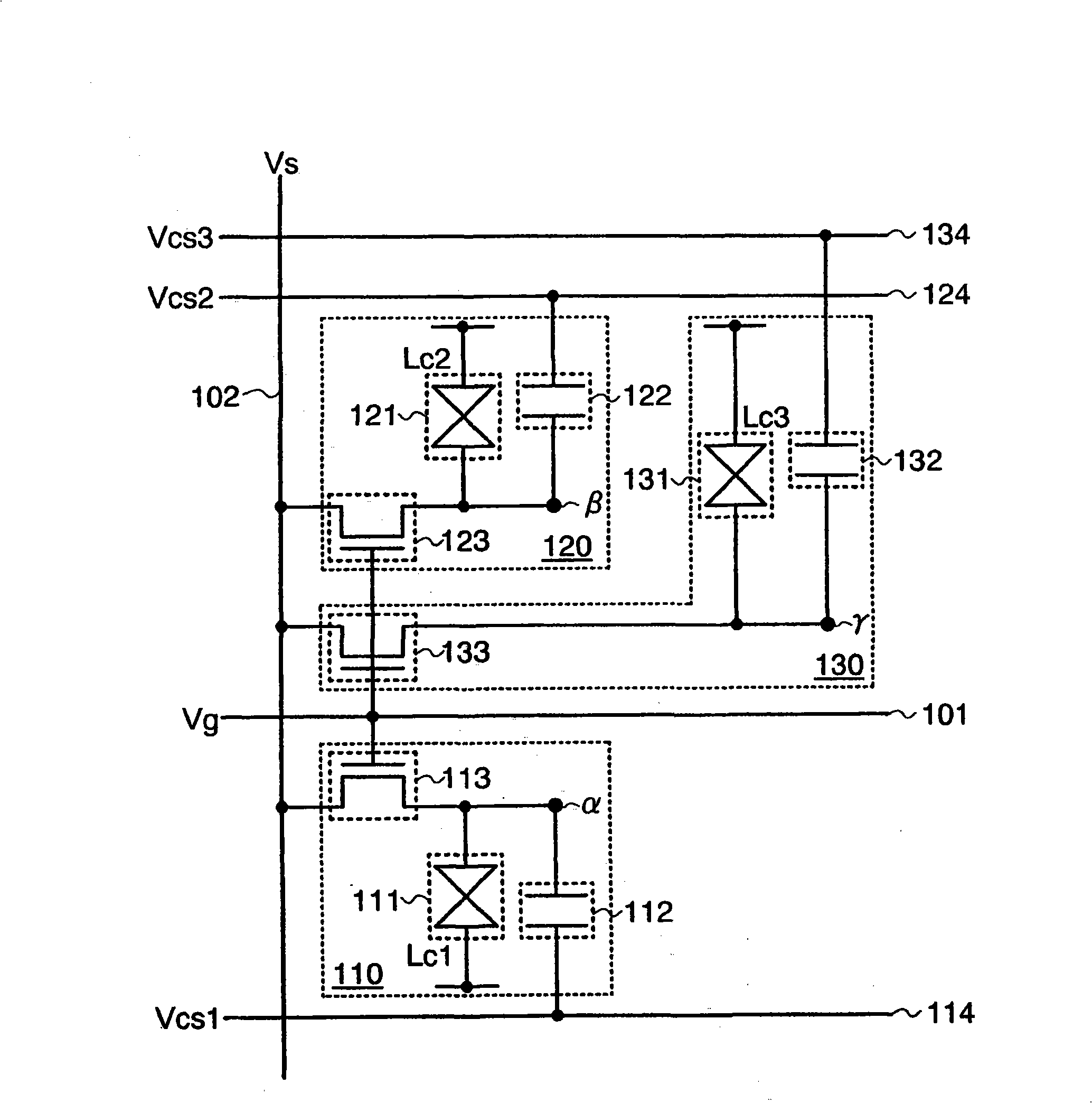
[0171] The structure of the display device shown in this embodiment mode is as follows: it has a plurality of pixels, and a plurality of sub-pixels are provided in each pixel. The structure of one pixel will be described using FIG. 1 .

[0172] The pixel shown in FIG. 1 shows a structure provided with three sub-pixels. The first sub-pixel 110 has a first liquid crystal layer 111 , a first capacitive element 112 , and a first transistor 113 . Likewise, the second sub-pixel 120 has a second liquid crystal layer 121, a second capacitive element 122, and a second transistor 123, and the third sub-pixel 130 has a third liquid crystal layer 131, a third capacitive element 132, and a third transistor 133. In addition, although a structure in which transistors are provided is shown here, other switching elements such as d...

Embodiment approach 2

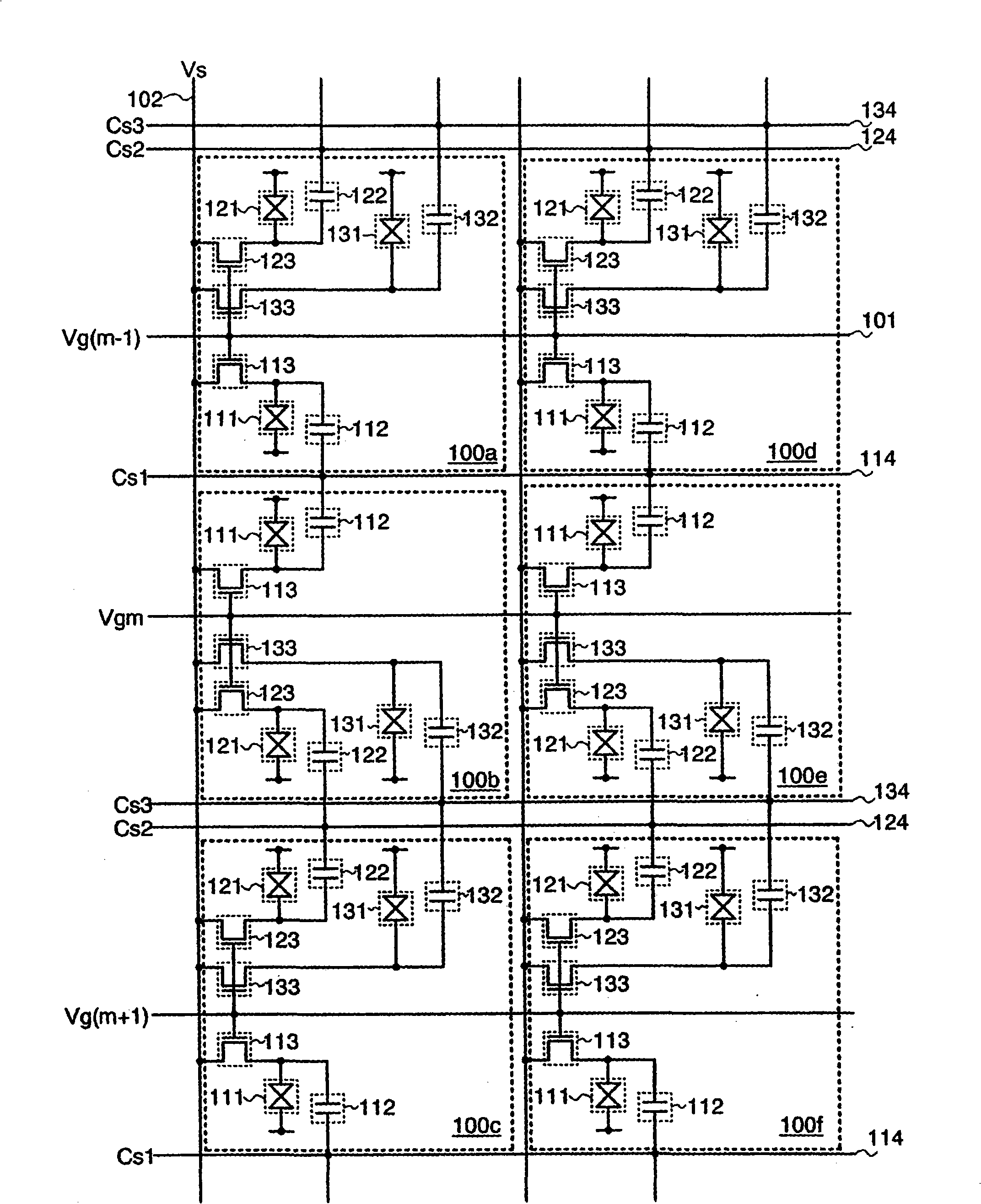
[0234] In this embodiment, a configuration of a display device different from the above-described embodiments will be described with reference to the drawings. Specifically, a description will be given of a configuration in which the scanning line and the third capacitance wiring are provided in common among the configurations shown in the above-mentioned embodiments.

[0235] FIG. 4 shows the pixel structure of the display device shown in this embodiment mode. In addition, FIG. 4 shows a structure in which three sub-pixels are respectively provided in the plurality of pixels 100a to 100f. Specifically, the first liquid crystal layer 111, the first capacitive element 112, and the first transistor 113 are provided in the first sub-pixel, and the second liquid crystal layer 121, the second capacitive element 122, and the second liquid crystal layer 121 are provided in the second sub-pixel. and the second transistor 123, and the third liquid crystal layer 131, the third capaciti...


PUM


Abstract

The target of this invention is to provide a display device in which a viewing angle characteristic is improved by providing a plurality of sub-pixels to one pixel. Alternatively, to provide a display device in which an aperture ratio is suppressed even when a plurality of sub-pixels is provided. A pixel including first sub-pixel, a second sub-pixel, and a third sub-pixel, a scanning line, a signal line, a first capacitor wiring, a second capacitor wiring and a third capacitor wiring are provided. Pixel electrodes each electrically connected to one electrode of the first to third capacitor elements, and the first to third capacitor wirings, respectively, are provided to the first to third sub-pixels electrodes, respectively. Potentials of the first capacitor wiring and the second capacitor wiring are changed and a potential of the third capacitor wiring is kept almost constant.

Description

technical field [0001] The present invention relates to a thing, a method, or a method of making a thing. In particular, the present invention relates to a display device or a semiconductor device. More specifically, the present invention relates to a display device provided with a plurality of sub-pixels in a pixel. Background technique [0002] In recent years, thin display devices such as liquid crystal display devices have been widely used in displays of mobile phones, TVs, and the like. In particular, liquid crystal display devices have excellent characteristics such as high definition, thin profile, and low power consumption, and their market scale is expanding. On the other hand, there is an increasing demand for enhancement of the functions of these display devices, for example, liquid crystal display devices with wide viewing angles and high image quality are expected. [0003] As a technique for improving the viewing angle characteristics, a method of improving ...

Claims


Application Information

Patent Timeline
Patent Type & Authority Applications(China)
IPC IPC(8): G02F1/1362G09G3/36
CPCG09G3/2025G02F2001/134345G09G2340/16G09G2320/0252G02F1/13624G09G2300/0426G09G2310/024G09G2300/0443G09G2300/0465G09G2310/0251G09G3/3659G09G2320/028G09G3/3607G09G2320/0673G09G2340/0435G09G3/3655G09G2320/0276G09G3/342G09G2320/0261G02F1/134345
Inventor 木村肇
Owner SEMICON ENERGY LAB CO LTD
Learn More