Flat display device with test structure

A flat display and test pad technology, applied in optics, instruments, electrical components, etc., can solve the problems of reducing product output rate, particle pollution products, increasing production costs, etc.

Active Publication Date: 2008-12-03
AU OPTRONICS CORP
View PDF0 Cites 37 Cited by
  • Summary
  • Abstract
  • Description
  • Claims
  • Application Information

AI Technical Summary

Problems solved by technology

However, during the laser cutting process, particles will contaminate the product, reducing the output rate of the product, and the laser cutting machine required for the process will increase the production cost

Method used


Image

  • Flat display device with test structure
  • Flat display device with test structure
  • Flat display device with test structure

Examples


Embodiment Construction

[0048] In order to make the present invention clearer and easier to understand, the following is a detailed description of the embodiment of the flat-panel display device with test structure according to the present invention and the accompanying drawings, but the provided embodiments are not intended to limit the scope of the present invention. scope.

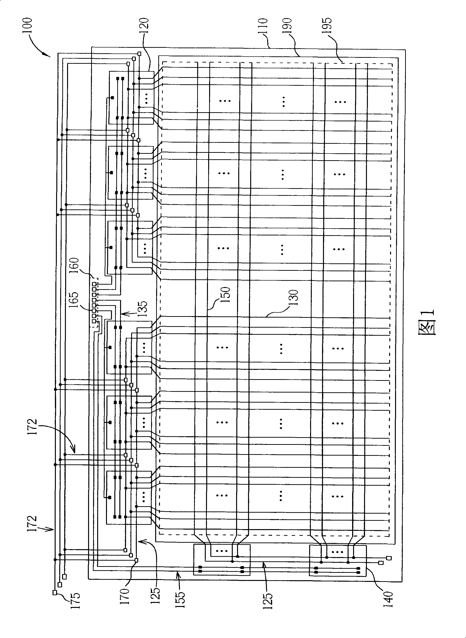
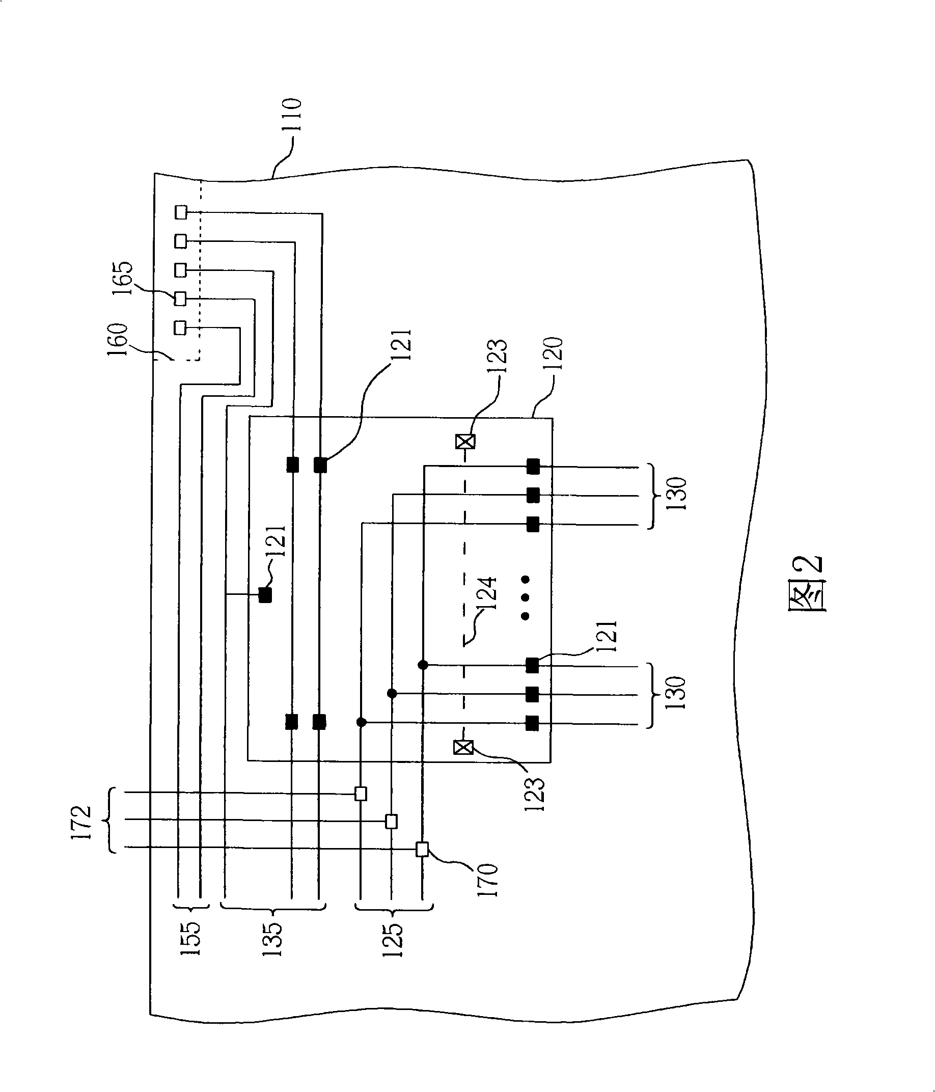
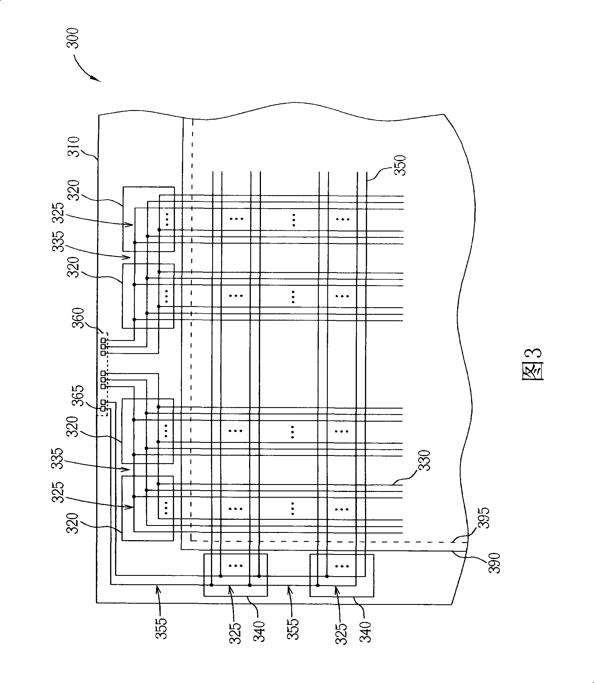
[0049] FIG. 3 is a schematic diagram of a flat-panel display device with a testing framework according to a first embodiment of the present invention. As shown in FIG. 3 , the flat panel display device 300 includes a lower substrate 310 , an upper substrate 390 , and a liquid crystal layer (not shown) sandwiched between the lower substrate 310 and the upper substrate 390 . The upper substrate 390 is a color filter for enabling the flat panel display device 300 to display color images. The lower substrate 310 includes a flexible printed circuit board bonding area 360, a plurality of source driver chip configuration regions 320...


PUM


Abstract

The invention discloses a plane display device provided with a testing mechanism and used for avoiding that a short-circuit wiring is arranged in an outer-pin landing zone to limit a bus-array wiring area. The plane display device mainly comprises a substrate provided with a plurality of driving-chip arrangement zone, a plurality of signal cables and transmitting cables which are arranged on the substrate, and a plurality of short-circuit wires arranged in the driving-chip arrangement zones. Each short-circuit wire is respectively coupled with a corresponding signal cable and a corresponding transmitting cable. Moreover, a plurality of transistors can be arranged in each driving-chip arrangement zone to control the signal connection between the short-circuit wires and signal cables and also control the signal connection between the short-circuit wires and transmitting cables so as to avoid a laser cutting program of the manufacturing process of the plane display device to reduce the manufacturing cost.

Description

technical field [0001] The present invention relates to a flat display device, in particular to a flat display device with a testing structure. Background technique [0002] Flat Panel Display (FPD) is currently the main popular display, and liquid crystal display (LCD) is widely used in computer screens, mobile phones, personal digital assistants ( PDA), flat-screen TV and other electronic products. The working principle of the liquid crystal display device is to change the arrangement state of the liquid crystal molecules in the liquid crystal layer by changing the voltage difference between the two ends of the liquid crystal layer, so as to change the light transmittance of the liquid crystal layer, and cooperate with the light source provided by the backlight module to display images. [0003] FIG. 1 is a prior art flat panel display device with a testing framework. As shown in FIG. 1 , the flat panel display device 100 includes a lower substrate 110 and an upper subst...

Claims


Application Information

Patent Timeline
Patent Type & Authority Applications(China)
IPC IPC(8): G02F1/1362G02F1/13H01L27/12H01L29/786
Inventor 刘俊欣陈勇志刘柏源蔡宗廷
Owner AU OPTRONICS CORP
Why Eureka
Try Eureka