Test platform and method for testing PC board

A test platform and test printing technology, which is applied in the direction of electronic circuit testing, etc., can solve the problems of high test cost, inability to test, and long test platform setup cycle, so as to achieve the effect of simple test process and avoid long setup cycle

Inactive Publication Date: 2008-12-31
SHENZHEN COSHIP ELECTRONICS CO LTD
View PDF0 Cites 28 Cited by
  • Summary
  • Abstract
  • Description
  • Claims
  • Application Information

AI Technical Summary

Problems solved by technology

[0004] It can be seen that since the setting of the placement table is set for the PCB of the 3.5-inch GPS device, and the current and voltage meter is connected to the pre-set test point, the test point is also selected for the PCB of the 3.5-inch GPS device, only the 3.5-inch Only when the PCB of the inch GPS device is correctly placed on the placement platform can the PCB be tested through the test points set by the placement platform, so this test platform cannot test other types of PCBs
Therefore, different types of GPS devices need to set up different test platforms to test them. Even after the GPS device undergoes a PCB revision, due to the change of its test points, the original PCB test platform of the GPS device cannot test the revised PCB.
When this test platform tests the PCB of a 3.5-inch GPS device, the tester needs to perform the test manually, and the test parameters need to be read by the tester himself and determine the test result. In the manual test process, the PCB may be damaged due to misoperation. Possibility, the test is cumbersome and requires relatively high skill requirements for testers
[0005] In summary, the current test platform can only be used for different types of PCBs that implement a certain function, but cannot test all PCBs, which is not universal.
Such testing will lead to the need to set up a corresponding PCB test platform to test a type of PCB, which brings many disadvantages: the test platform setup cycle is relatively long, the test cost is high and the test efficiency is low, etc.
In addition, when using the set test platform to test the corresponding PCB, the testers manually test and determine the test results according to the test parameters, so there may be misjudgment or misoperation during the test process.

Method used


Image

  • Test platform and method for testing PC board
  • Test platform and method for testing PC board
  • Test platform and method for testing PC board

Examples


Embodiment Construction

[0036] In order to make the object, technical solution and advantages of the present invention clearer, the present invention will be further described in detail below with reference to the accompanying drawings and examples.

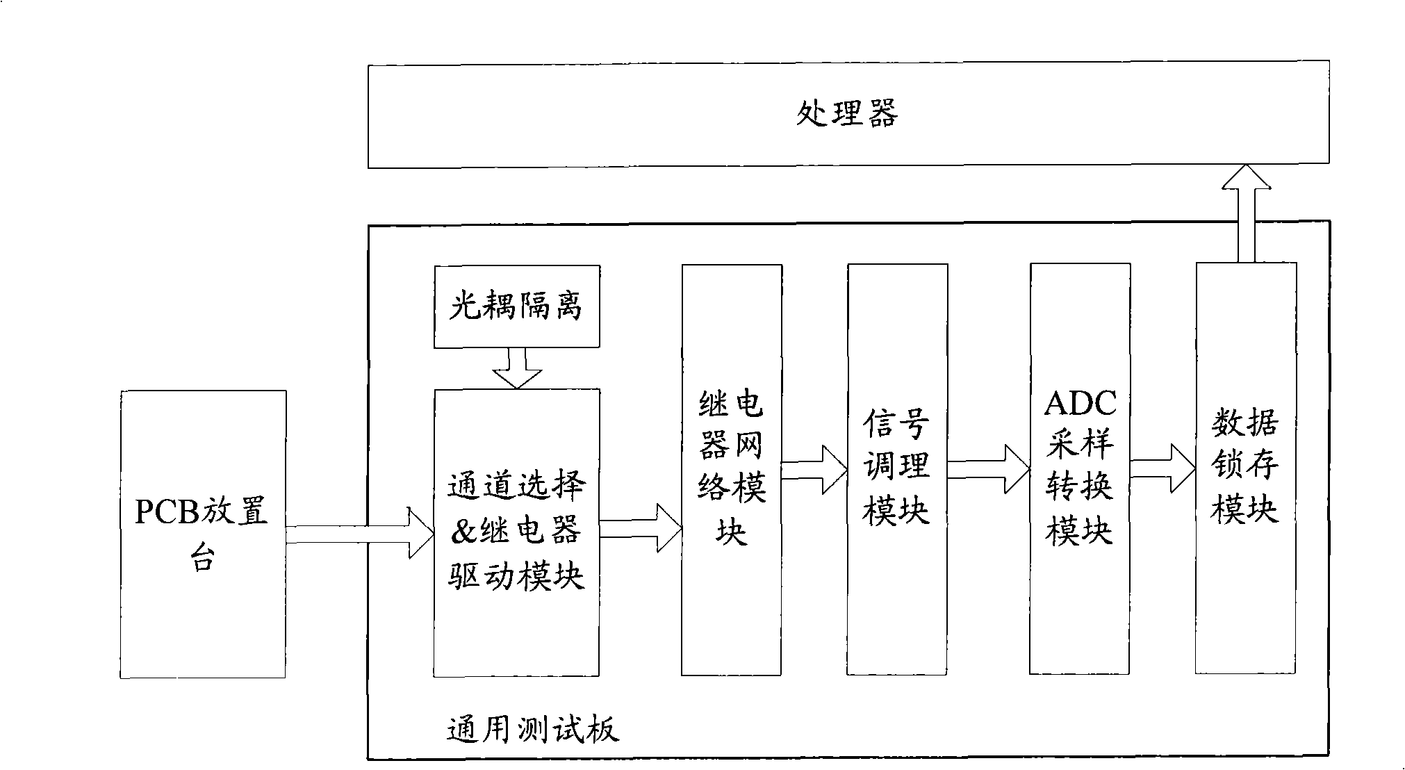
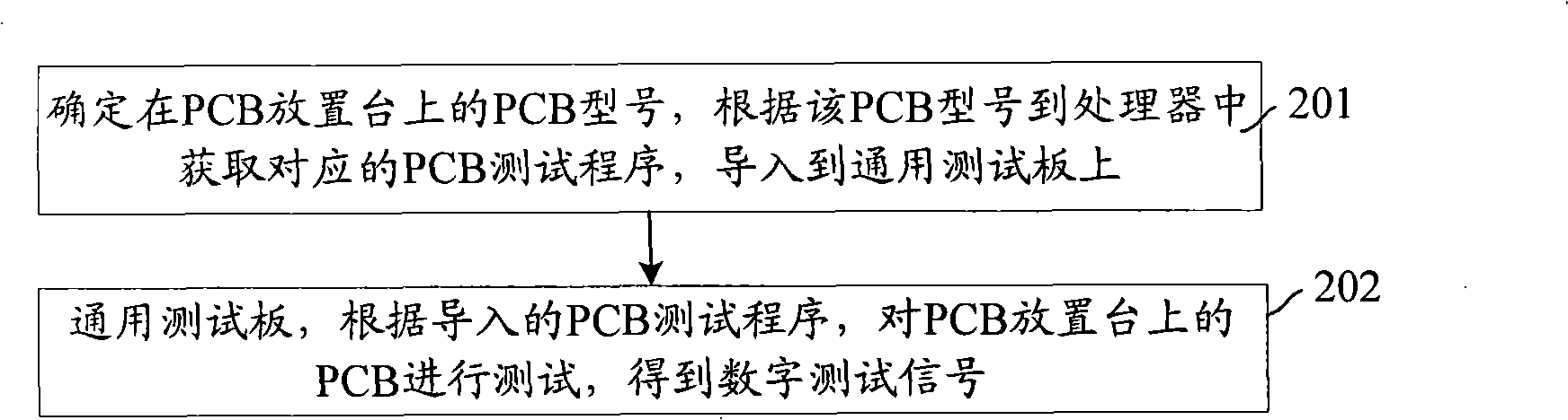
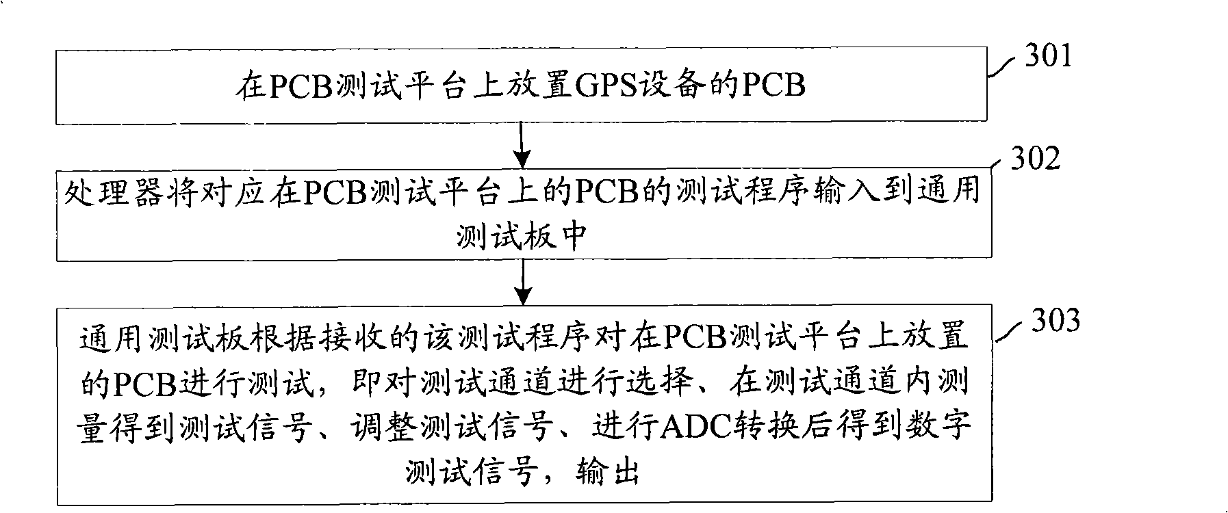
[0037] In order to avoid the various shortcomings caused by using different test platforms for PCBs with different functions or different types of PCBs with the same function as in the prior art, the present invention provides PCBs with different functions or different types of PCBs with the same function. A common test bench is set up. When testing the PCB, the corresponding test program will be run on the test platform, and the test platform will set the corresponding test points for the PCB on the placement table according to the test program. After testing the PCB on the placement table through the set test points, the The obtained test parameters are compared with the set test standard to obtain the final test result.

[0038] figure 1 The schema...


PUM


Abstract

The invention discloses a test platform and a method for testing a printed circuit board, wherein, the test platform comprises: a processor, a universal test board and a placing table of the printed circuit board PCB, wherein, the processor is used for storing test procedures, when in test of the PCB, the processor introduces the test procedure corresponding to the PCB to the universal test board and receives digital test parameters or test result sent by the universal test board; the universal test board is used for carrying out the test of the corresponding test point of the PCB which is arranged on the placing table of the PCB according to the test procedure received from the processor and outputting the obtained digital test parameters or the test result to the processor after the completion of the test; and the placing table of the PCB is used for placing the PCB. Therefore, the test platform and the method can realize the test of the PCB with the same function and different types or the PCB with the different functions, thereby avoiding the shortcomings of longer setting period of the test platform, high test cost and low test efficiency.

Description

technical field [0001] The invention relates to the processing field of printed circuit boards (PCB, Printed Circuit Board), in particular to a testing platform and method for testing PCBs. Background technique [0002] With the development of circuit technology, PCB can realize various functions, such as using PCB to manufacture Global Positioning System (GPS, Global Positioning System) equipment for positioning and so on. When a PCB that implements a certain function is manufactured, it is necessary to test the manufactured PCB, and determine whether it meets the design standard according to the parameters obtained from the test. When testing a PCB, a test platform and a test method are required. Often, different test platforms and test methods are set for PCBs with different functions. Even for different types of PCBs that implement the same function, such as different types of GPS devices, the test platforms and test methods set are different. [0003] Give an example ...

Claims


Application Information

Patent Timeline
Patent Type & Authority Applications(China)
IPC IPC(8): G01R31/28
Inventor 刘志军
Owner SHENZHEN COSHIP ELECTRONICS CO LTD
Why Eureka
Try Eureka