Charge pump drive circuit

A driving circuit and charge pump technology, which is applied in the field of high-frequency noise, can solve the problems of increasing circuit size and chip size, and achieve the effect of suppressing the increase of circuit size and reducing high-frequency noise

Inactive Publication Date: 2009-01-14
RENESAS ELECTRONICS CORP
View PDF1 Cites 11 Cited by
  • Summary
  • Abstract
  • Description
  • Claims
  • Application Information

AI Technical Summary

Problems solved by technology

Therefore, according to the charge pump drive circuit described in Japanese Laid-Open Patent Application (JP-P2006-340436A), there is a problem of increasing circuit size and chip size

Method used


Image

  • Charge pump drive circuit
  • Charge pump drive circuit
  • Charge pump drive circuit

Examples


Embodiment Construction

[0021] The invention will now be described with reference to illustrative embodiments. Those skilled in the art will recognize that many alternative embodiments can be accomplished using the teachings of the present invention and that the invention is not limited to the embodiments illustrated for explanatory purposed.

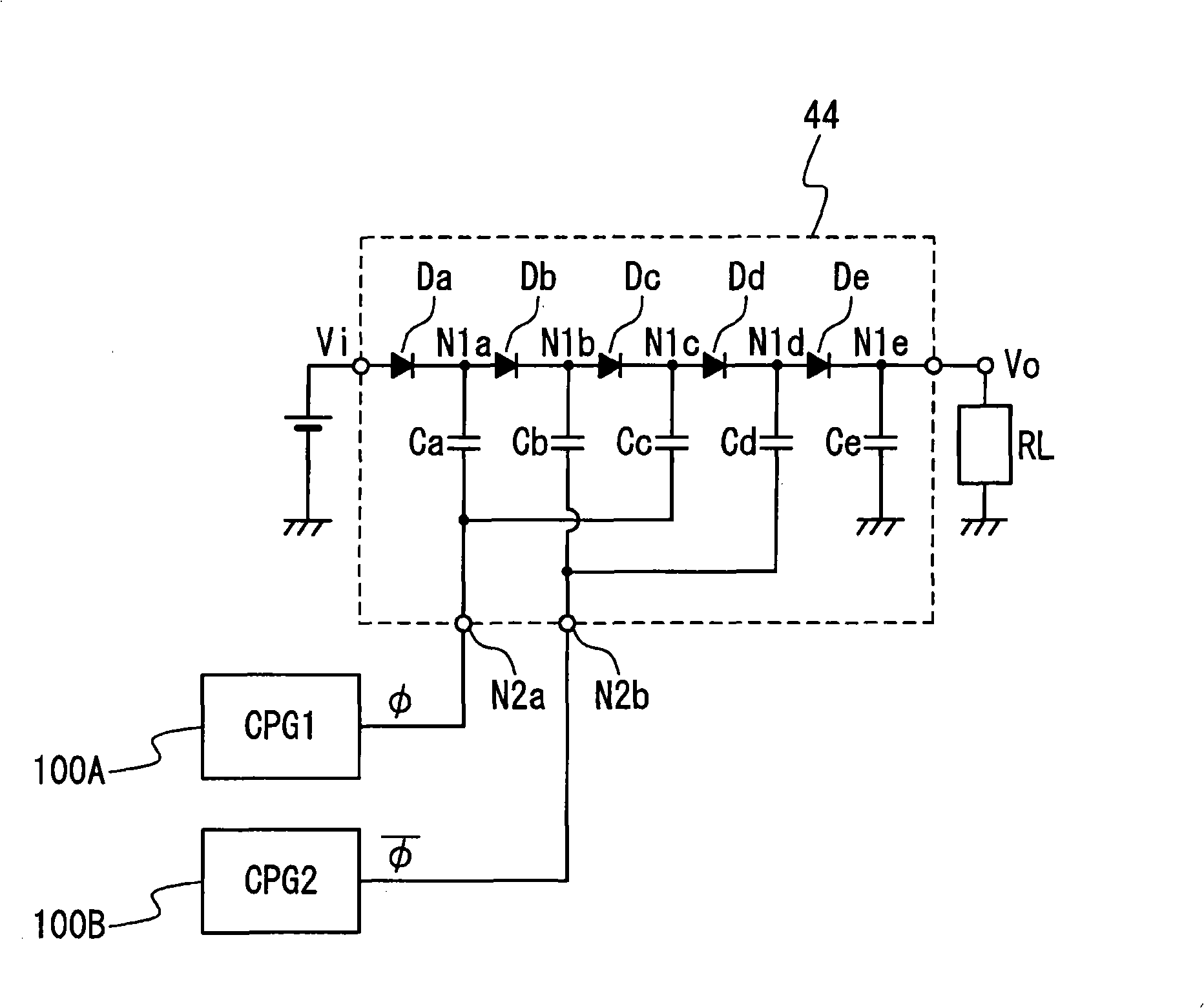
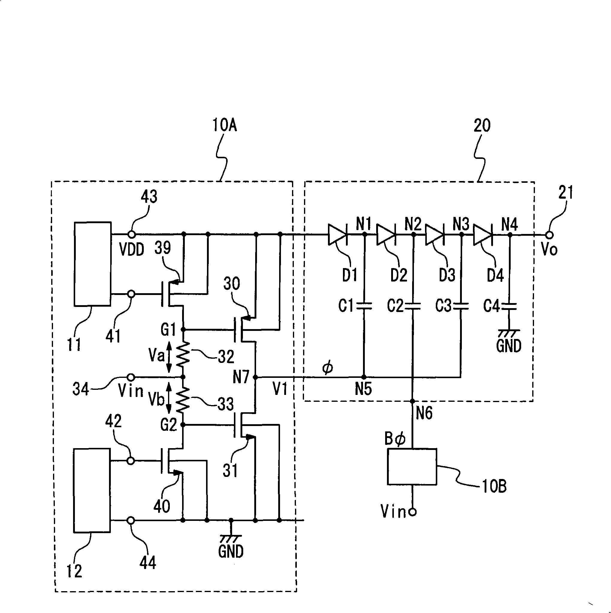
[0022] figure 2 is a circuit diagram of the semiconductor device according to the first embodiment of the present invention. In this embodiment, as an example of a circuit of a semiconductor device, a booster circuit for boosting the power supply voltage VDD to an output voltage that is four times the power supply voltage VDD is described.

[0023] (structure)

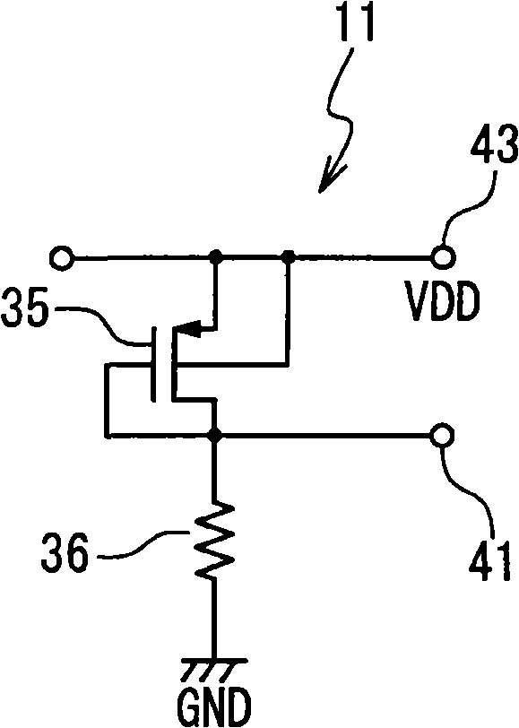
[0024] refer to Figure 2 to Figure 4 , the semiconductor device (booster circuit) according to the present embodiment will be explained. refer to figure 2 , the semiconductor device according to the embodiment of the present invention includes charge pump driving circuits 10A and 10B and a charge...


PUM


Abstract

A charge pump drive circuit includes a first MOSFET (Metal Oxide Semiconductor Field Effect Transistor) and a second MOSFET. The first MOSFET and the second MOSFET are different in channel type and provided to form a complementary inverter circuit. The complementary inverter circuit drives a charge pump circuit based on an input potential inputted to an input terminal. A first gate of the first MOSFET and a second gate of the second MOSFET are connected to the input terminal such that a potential at the first gate is different from a potential at the second gate.

Description

technical field [0001] The present invention relates to a charge pump driving circuit, a semiconductor device using the charge pump driving circuit, and a voltage conversion method, and more particularly, to reducing high frequency noise in a charge pump circuit for raising or lowering a direct current (DC) voltage. Background technique [0002] A Dickson type charge pump circuit is known as a charge pump circuit for stepping up or down a DC voltage. One example of such a charge pump is disclosed in Japanese Laid-Open Patent Application (JP-P2006-340436A). Referring to FIG. 1 , a description will be given of a voltage boosting circuit using a Dickson type charge pump circuit. [0003] Referring to FIG. 1, a charge pump circuit for a boost circuit includes five diodes Da to De and five capacitors Ca to Ce connected in series between a power supply Vi and an output terminal Vo. Ends of the capacitors Ca to Ce (or nodes N1a to N1e ) are connected to anodes of the diodes Da to...

Claims


Application Information

Patent Timeline
Patent Type & Authority Applications(China)
IPC IPC(8): H02M3/07
CPCH02M3/073
Inventor 本多悠里
Owner RENESAS ELECTRONICS CORP
Why Eureka
Try Eureka