Preparation method for LED and tool for preparing the LED

A technology of light-emitting diodes and fixtures, applied in semiconductor/solid-state device manufacturing, electrical components, electric solid-state devices, etc., can solve the problems of complicated steps and cost of materials, so as to reduce the manufacturing process, reduce the manufacturing process, and reduce the manufacturing cost Effect

Inactive Publication Date: 2009-01-28
EVERLIGHT ELECTRONICS
View PDF0 Cites 2 Cited by
  • Summary
  • Abstract
  • Description
  • Claims
  • Application Information

AI Technical Summary

Problems solved by technology

[0009] According to the above, the existing manufacturing method of light-emitting diodes not only has complicated steps in the process, but also, in order to manufacture a plurality of light-emitting diodes at one time (the general rack row 120 can produce twenty or thirty light-emitting diodes), It is necessary to sacrifice a lot of bracket waste to form a predetermined number of LED brackets. Under mass production, the cost of materials is quite high, and this has been an insurmountable problem in the industry for a long time.

Method used


Image

  • Preparation method for LED and tool for preparing the LED
  • Preparation method for LED and tool for preparing the LED
  • Preparation method for LED and tool for preparing the LED

Examples


Embodiment Construction

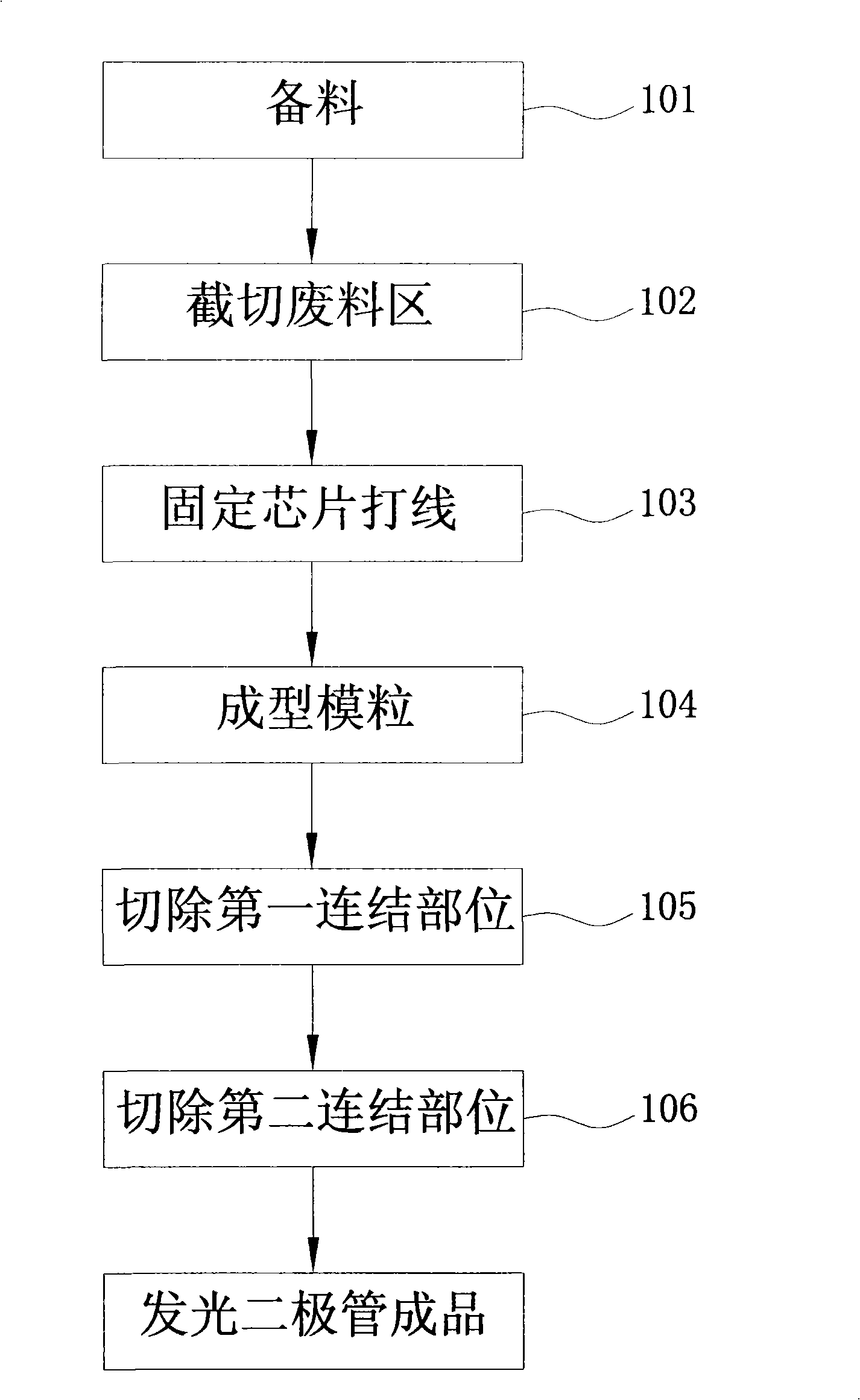
[0056] refer to Figure 8 , is a flowchart of the steps of an embodiment of the present invention.

[0057] The preparation method of the light-emitting diode of the present invention comprises the following manufacturing steps:

[0058] Step (1): Such as process 201 and reference Figure 9 and Figure 10 , forming a plurality of first brackets 210 and a plurality of second brackets 220 respectively.

[0059]Step (2): As shown in the process 202 and referring to FIG. 11 , the first brackets 210 and the second brackets 220 are fixed in pairs on the plurality of first mounting parts 310 and the plurality of On the loading portion 320 , a first bracket 210 and a second bracket 220 adjacent to each other form a bracket group 230 . And a clamp 400 is coupled to the jig body 300 to fix the first brackets 210 and the second brackets 220 .

[0060] Step (3): such as process 203 and reference Figure 12 , a chip 240 is fixed on a bowl groove 221 of the second bracket 220, and a w...


PUM


Abstract

The invention discloses a method and a jig for manufacturing a light emitting diode (LED). The method comprises the following steps: a plurality of first supports and second supports are respectively formed and fixed on the jig in pairs, so that adjacent first support and second support are formed into a support group; then a chip is fixed on one of the supports to carry out routing operation; moreover, grain forming operation is carried out on each pair of support groups, thereby forming an LED finished product.

Description

technical field [0001] The invention relates to a light-emitting diode, and in particular to a method for manufacturing a light-emitting diode with simple process, no waste material, and reduced manufacturing cost and a jig for manufacturing the light-emitting diode. Background technique [0002] refer to figure 1 A flow chart of an existing light-emitting diode manufacturing method, comprising the following steps: [0003] Step (1): Refer to figure 1 The process 101 of FIG. 2 and the plan view of FIG. 2 prepare a stent substrate 100 with a predetermined area. [0004] Step (2): Refer to figure 1 3, the unnecessary waste area 110 in FIG. The bracket row 120 includes a plurality of first brackets 121 , a plurality of second brackets 122 , a first connecting portion 123 and a second connecting portion 124 . [0005] Step (3): Refer to figure 1 The process 103 of FIG. 4 and the plan view of FIG. 4 are used to carry out the bonding operation, and a light-emitting diode chi...

Claims


Application Information

Patent Timeline
Patent Type & Authority Applications(China)
IPC IPC(8): H01L33/00H01L21/50
CPCH01L2224/48247H01L2224/97H01L2924/181H01L2924/00012
Inventor 沈素靖庄建德
Owner EVERLIGHT ELECTRONICS
Why Eureka
Try Eureka