Liquid crystal cell substrate fabrication method, liquid crystal cell substrate, and liquid crystal display device
A technology of liquid crystal display device and liquid crystal unit, applied in liquid crystal materials, chemical instruments and methods, optical components, etc., which can solve the problems of rising cost, increased number of processes, difficulties, etc., and achieve excellent productivity, correct optical compensation, and improved color viewing angle The effect of the characteristic
- Summary
- Abstract
- Description
- Claims
- Application Information
AI Technical Summary
Problems solved by technology
Method used
Image
Examples
Embodiment 1~3
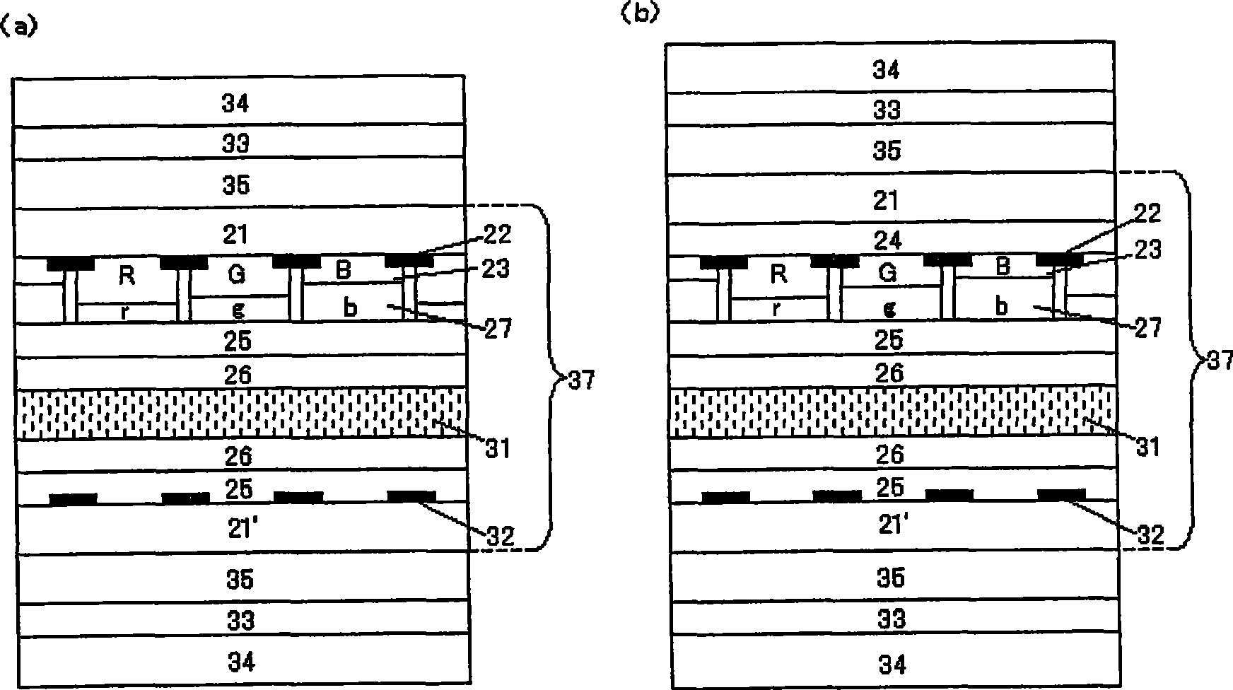
[0266]On the above-mentioned color filter 1 substrate, using a laminator (manufactured by Hitachi Industrias (Lamic II type)), the transfer materials of the above-mentioned Examples 1 to 3 were respectively heated at the above-mentioned 100° C. for 2 minutes on the substrate with rubber coating. Lamination was performed at a roll temperature of 130° C., a linear pressure of 100 N / cm, and a conveying speed of 2.2 m / min. After peeling off the temporary support and the alignment film, an optically anisotropic layer was provided on the color filter. At this time, the thickness of the optically anisotropic layer on each RGB pixel of the optically anisotropic layer differs based on the difference in thickness between the RGB pixels of the color filter, and is 3.15 μm on R, 2.75 μm on G, and 2.15 μm on B. μm. In addition, the delays Re(40) and Re(-40) on the RGB pixels are as follows.
[0267] For R, G, and B, retardation at λ of 611 nm, 545 nm, and 435 nm, respectively, was measure...
Embodiment 4~6
[0280] Except having used the color filter 2 board|substrate, it carried out similarly to Example 1, and provided the optically anisotropic layer on a color filter. At this time, the thickness of the optically anisotropic layer on each RGB pixel of the optically anisotropic layer differs based on the difference in thickness between the RGB pixels of the color filter, and is 3.15 μm on R, 2.75 μm on G, and 2.15 μm on B. μm.
[0281] In addition, the delays Re(40) and Re(-40) on the RGB pixels are as follows.
[0282] For R, G, and B, retardation at λ of 611 nm, 545 nm, and 435 nm, respectively, was measured.
[0283]
[0284] In addition, VA-LCD was prepared and evaluated in the same manner as in Example 1. As a result, there was almost no change in the black display, and no significant light leakage was observed at the corners. In addition, favorable contrast viewing angle characteristics were obtained, and the result that almost no color shift was observed at the time of...
Embodiment 7~9
[0286] Except having used the color filter 3 board|substrate, it carried out similarly to Example 1, and provided the optically anisotropic layer on a color filter. At this time, the thickness of the optically anisotropic layer on each RGB pixel of the optically anisotropic layer differs based on the difference in thickness between the RGB pixels of the color filter, and is 3.15 μm on R, 2.75 μm on G, and 2.15 μm on B. μm. In addition, the delays Re(40) and Re(-40) on the RGB pixels are as follows.
[0287] For R, G, and B, retardation at λ of 611 nm, 545 nm, and 435 nm, respectively, was measured.
[0288]
[0289] In addition, VA-LCD was prepared and evaluated in the same manner as in Example 1. As a result, there was almost no change in the black display, and no significant light leakage was observed at the corners. In addition, favorable contrast viewing angle characteristics were obtained, and the result that almost no color shift was observed at the time of black di...
PUM
| Property | Measurement | Unit |
|---|---|---|
| wavelength | aaaaa | aaaaa |
| illuminance | aaaaa | aaaaa |
| softening point | aaaaa | aaaaa |
Abstract
Description
Claims
Application Information


