Light-emitting diode and method for fabricant thereof
A technology of light-emitting diodes and light-emitting layers, which is applied to semiconductor devices, electrical components, circuits, etc., can solve the problems of reducing the back surface area, reducing heat release characteristics, cost issues, etc., and achieves suppressed operating voltage, high reliability, and high brightness Effect
- Summary
- Abstract
- Description
- Claims
- Application Information
AI Technical Summary
Problems solved by technology
Method used
Image

Examples
example 1
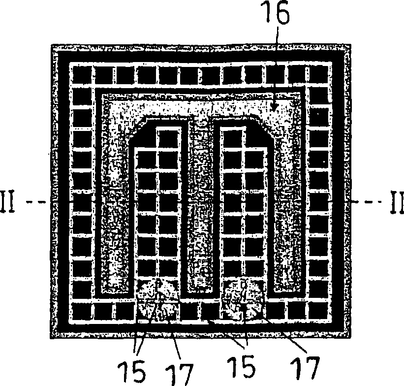
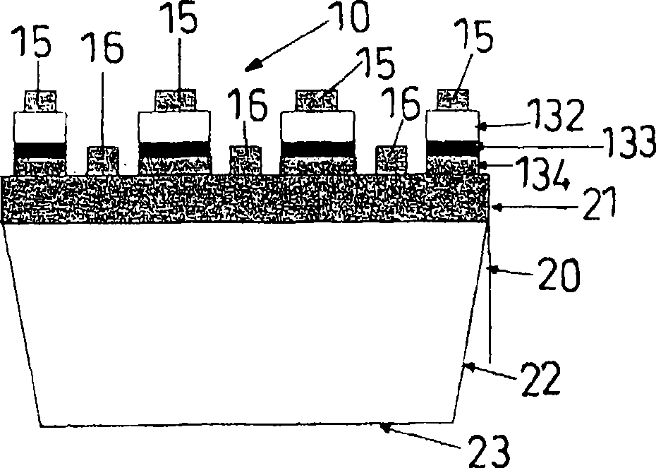
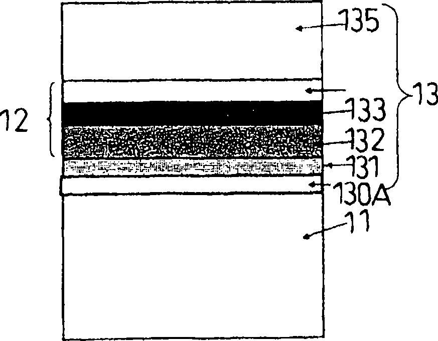
[0131] figure 1 and figure 2 The semiconductor light emitting diode 10 manufactured in Example 1 is schematically illustrated. figure 1 is a planar graph, and figure 2 is along figure 1 A cross-sectional view taken along line II-II. image 3 is a schematic cross-sectional view of the multilayer structure of the semiconductor epitaxial stacked structure used in the semiconductor light emitting diode 10 of Example 1, and Figure 4 is an example by bonding the substrate 14 to the image 3 A schematic cross-sectional view of a structure produced by a semiconductor epitaxial stacked structure.
[0132] The semiconductor light emitting diode 10 manufactured in Example 1 was a red light emitting diode (LED) having an AlGaInP light emitting portion 12 . It is made by bonding an epitaxial laminated structure formed on a semiconductor substrate 11 made of GaAs and a GaP substrate 14 .
[0133] The light-emitting diode 10 is manufactured by using an epitaxial wafer...
manufacture example 2
[0149] A semiconductor light emitting diode 10 of Example 2 was manufactured, which had the same structure as that of Example 1, but made a metal layer 24 of AuSn eutectic (melting point: 283° C.) formed on the back surface, as Figure 5 shown in .
[0150] The assembly with Figure 8 and Figure 9 A semiconductor light-emitting diode lamp (LED lamp) 1 of the structure schematically exemplified in FIG.
[0151] In the same manner as in Example 1, the semiconductor light emitting diode lamp 1 manufactured by using the semiconductor light emitting diode 10 of Example 2 was evaluated. The results are shown in Table 1 below. The forward voltage (Vf) during which a current of 500 mA flows in the forward direction is 2.4V. The intensity of light emission was able to reach a high brightness of 6430mcd, reflecting the fact that the heat release characteristics were further improved and the absorption of light by the Ag paste was eliminated.
example 3
[0161] A light emitting diode according to Example 3, which is another specific example of the second embodiment, will be described below by referring to the drawings.
[0162] Figure 10 and Figure 11 The semiconductor light emitting diode 10 of Example 3 is illustrated. Figure 10 is a planar graph, and Figure 11 is along Figure 10 A cross-sectional view taken along line XI-XI. Figure 12 is a schematic cross-sectional view of the multilayer structure of the semiconductor epitaxial stacked structure used in the light emitting diode 10 of Example 3, and Figure 13 is an example by bonding a GaP substrate 14 to Figure 12 A schematic cross-sectional view of a structure produced by a semiconductor epitaxial stacked structure.
[0163] The semiconductor light emitting diode 10 of Example 3 is a red light emitting diode (LED) having an AlGaInP light emitting portion 12, which is fabricated by bonding an epitaxial laminated structure provided on a semiconduc...
PUM
| Property | Measurement | Unit |
|---|---|---|
| Length | aaaaa | aaaaa |
| Length | aaaaa | aaaaa |
| Thickness | aaaaa | aaaaa |
Abstract
Description
Claims
Application Information
 - R&D
- Intellectual Property
- Life Sciences
- Materials
- Tech Scout
- Unparalleled Data Quality
- Higher Quality Content
- 60% Fewer Hallucinations
Browse by: Latest US Patents, China's latest patents, Technical Efficacy Thesaurus, Application Domain, Technology Topic, Popular Technical Reports.
© 2025 PatSnap. All rights reserved.Legal|Privacy policy|Modern Slavery Act Transparency Statement|Sitemap|About US| Contact US: help@patsnap.com