Switching apparatus, electric field applying method and switching system

A switching device and electric field direction technology, applied in circuits, relays, electrical components, etc., can solve problems such as insufficient displacement, damage to switch flatness, and increased cost, and achieve the effect of low resistance and good contact

Inactive Publication Date: 2005-12-14
PANASONIC CORP
View PDF3 Cites 0 Cited by
  • Summary
  • Abstract
  • Description
  • Claims
  • Application Information

AI Technical Summary

Problems solved by technology

[0009] However, in this form, there is also the following problem in manufacturing a practical finished product: the free end is warped under the residual stress at the time of film formation, thereby damaging the flatness of the switch (for example, refer to JP-A-11-340702 ( Figure 2-5 ) and JP-A-2000-348594 ( figure 1 ))
[0011] However, the amount of displacement improved by this method is not large enough, and the contact in the fixed end for generating the bending moment needs to be of a certain size, so that the real trial production is difficult and increases the cost
Therefore, this method is not suitable for mass production of actuators

Method used


Image

  • Switching apparatus, electric field applying method and switching system
  • Switching apparatus, electric field applying method and switching system
  • Switching apparatus, electric field applying method and switching system

Examples


no. 1 example

[0057] A first embodiment of the present invention will be described below with reference to the drawings.

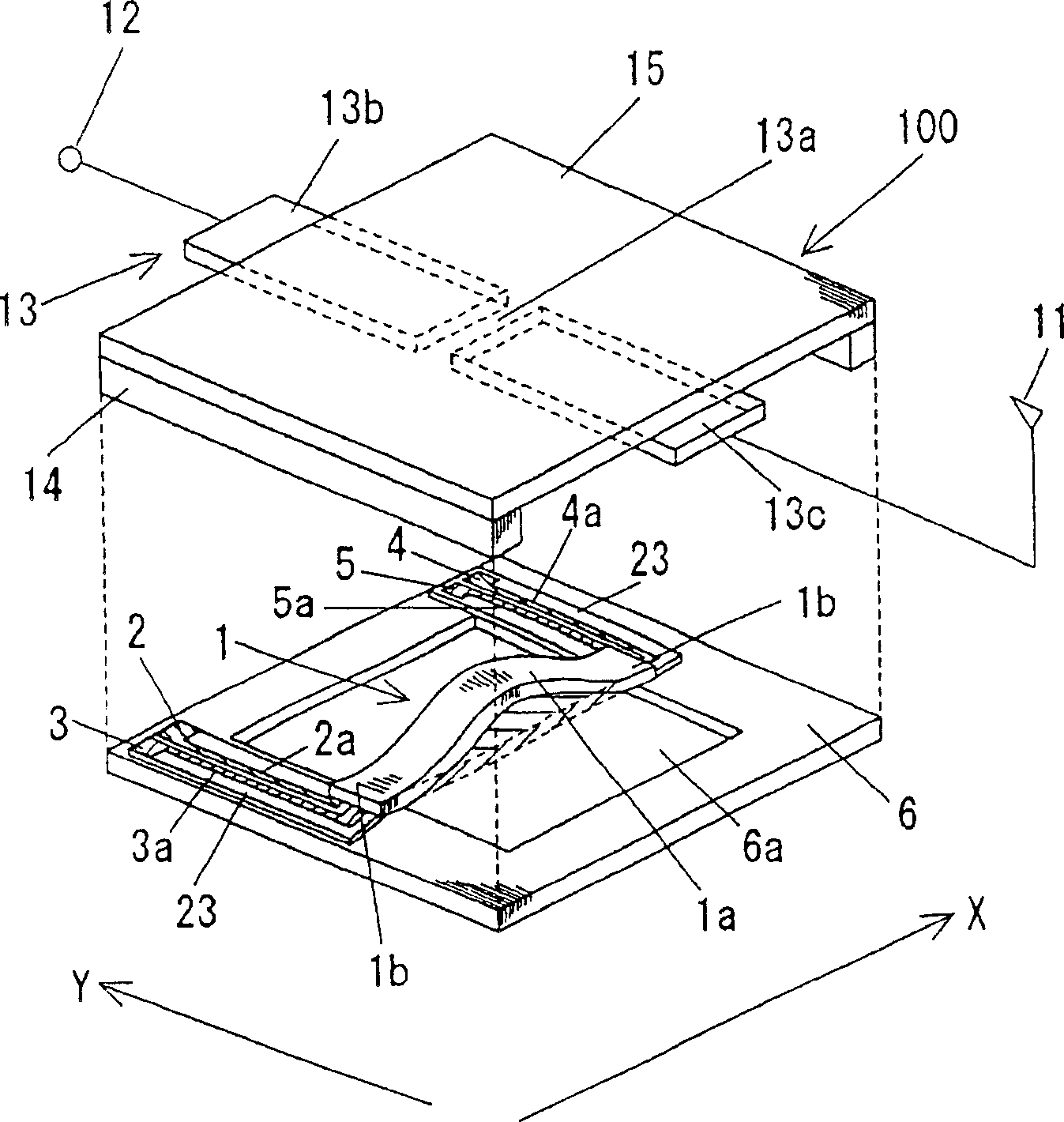
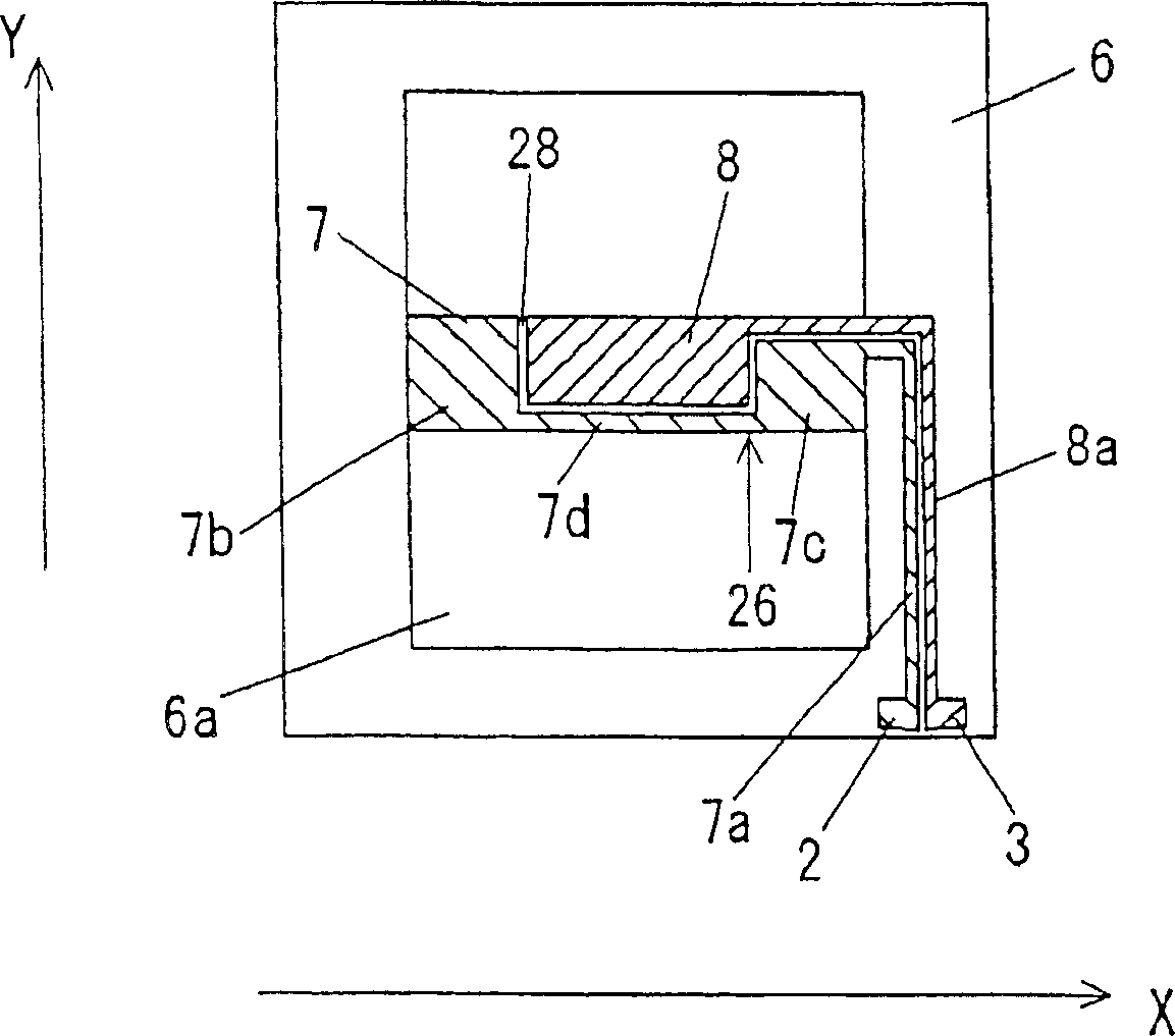
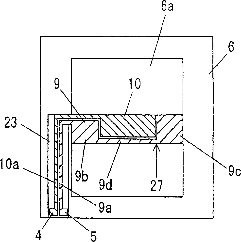
[0058] figure 1 is an exploded perspective view showing the configuration of the switchgear in the first embodiment of the present invention. figure 2 is a structural view showing the substrate-side electrode (lower electrode) of the switching device in the first embodiment, image 3 is a structural view showing the gap electrode side electrode (upper electrode) of the switching device in the first embodiment, Figure 5 is an exploded side view of the actuator at rest including the switching device of the first embodiment, .

[0059] In these drawings, reference numeral 100 is a switching device including a substrate 6 , an actuator 1 , an upper substrate 15 , a gap electrode 13 and a spacer 14 .

[0060] The following will refer to Figure 1-3 and Figure 5 The configuration of the switchgear is described in detail.

[0061] The substrate 6 is formed of an MgO m...

no. 2 example

[0096] Next, we will refer to Figure 7 and 8 A second mode for carrying out the present invention will be described. Figure 7 is the front view of the switchgear in the second mode, Figure 8 is a perspective view of the switchgear in the second mode. The switching device in this mode comprises a first movable part 60 , a second movable part 61 and a third movable part 62 . The two ends of the first movable part 60 are connected to the second movable part 61 and the third movable part 62 near the middle positions of the second movable part 61 and the third movable part 62 . The connected first movable part 60, second movable part 61 and third movable part 62 form a letter "H" shape. Only the second movable portion 61 and the third movable portion 62 are provided with the fixed portion 60 b connected to the base plate 6 , and the fixed portion 60 b is connected to the base plate 6 . By combining the three movable parts in this way, the amount of displacement can be made ...


PUM


Abstract

A switch device having an electrode pair including a first electrode and a third electrode with a piezoelectric element interposed therebetween, and a second electrode and a fourth electrode that are electrically insulated from and adjacent to the first electrode and the third electrode. An electrode pair of electrodes generates an electric field in a first direction between the first electrode and the third electrode, while generating an electric field in a second direction between the second electrode and the fourth electrode.

Description

technical field [0001] The present invention relates to a switching device, and more particularly, to a switching device having a small insertion loss in a high frequency band such as a frequency band higher than GHz, an electric field applying method thereof, and a switching system. Background technique [0002] Recently, telecommunication systems, especially mobile phones or wireless cellular phones are being remarkably developed. For example, in a TDMA type communication system, transmission and reception of RF signals in a GHz high-frequency band are performed through an antenna. In these systems, antennas are often used alternately as output for the transmit phase and input for the receive phase. Therefore, the performance requirements for switches in such systems are sufficiently low resistance when connected and high enough isolation when disconnected. If the resistance is not small enough at the time of connection, insertion loss will be caused by the generation of...

Claims


Application Information

Patent Timeline
Patent Type & Authority Applications(China)
IPC IPC(8): H01H57/00
Inventor 水山洋右松原正吾堀尾英明
Owner PANASONIC CORP
Why Eureka
Try Eureka