Microwave plasma CVD system

A microwave plasma, microwave technology, used in crystal growth, from chemically reactive gases, semiconductor/solid state device manufacturing, etc.

Inactive Publication Date: 2009-04-15
SUMITOMO ELECTRIC IND LTD
View PDF3 Cites 25 Cited by
  • Summary
  • Abstract
  • Description
  • Claims
  • Application Information

AI Technical Summary

Problems solved by technology

In other words, it is difficult to say that plasma position control under conditions capable of producing large-area high-quality diamond films can be satisfactorily performed.

Method used


Image

  • Microwave plasma CVD system
  • Microwave plasma CVD system
  • Microwave plasma CVD system

Examples


Embodiment 1

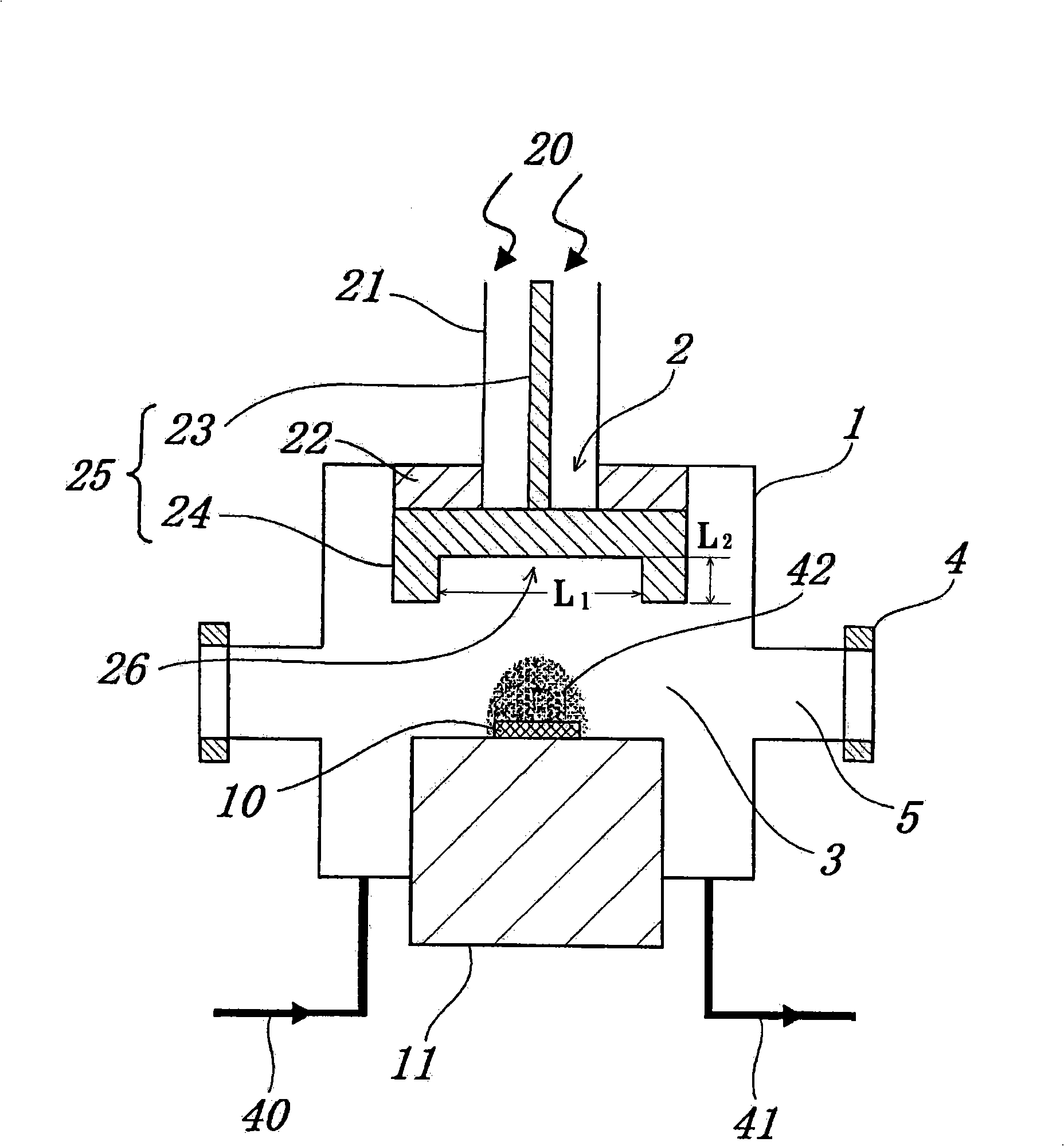
[0061] manufacture figure 1 The microwave plasma CVD device is shown, and an attempt is made to synthesize semiconducting diamond. The microwave 20 is in the 2.45GHz frequency band (band), and for the size of the concave portion 26, the diameter (L 1 ) is made equal to the length of 1 wavelength, and the depth from the surface facing the center of the vacuum chamber to the deepest part of the recess (L 2 ) is made equal to 1 / 5 wavelength. As materials of the device constituent parts, stainless steel was used for the metal part and quartz was used for the dielectric part. As the substrate 10, a 2×2×0.3 mmt high temperature and high pressure synthetic IIa(111) single crystal substrate placed in the center in a square shape and a Base material for molybdenum disks. Hydrogen, methane and phosphine are introduced into the interior of the vacuum chamber 3 from the raw material gas supply pipe 40, and the flow rates of the hydrogen, methane and phosphine are adjusted by mass flo...

Embodiment 2

[0065] The same experiment as in Example 1 was performed except that, for the recess 26, a recess manufactured by selecting any of 1 / 3 wavelength, 1 / 2 wavelength, 1 wavelength, 3 / 2 wavelength, and 5 / 3 wavelength was used. One dimension is taken as the diameter at the surface facing the center of the vacuum chamber (L 1), and select any size of 1 / 20 wavelength, 1 / 10 wavelength, 1 / 3 wavelength, 1 / 2 wavelength and 3 / 5 wavelength as the depth from the surface facing the center of the vacuum chamber to the deepest part of the concave portion ( L 2 ), obtain substantially the same result as in Example 1. In particular, stable semiconducting diamond synthesis was achieved without any observed plasma flickering in experiments using a recess in which the diameter at the surface facing the center of the vacuum chamber (L 1 ) in the 1 / 2 to 3 / 2 wavelength range, and the depth from the surface facing the center of the vacuum chamber to the deepest part of the recess (L 2 ) is 1 / 10 to 1 / ...

Embodiment 3

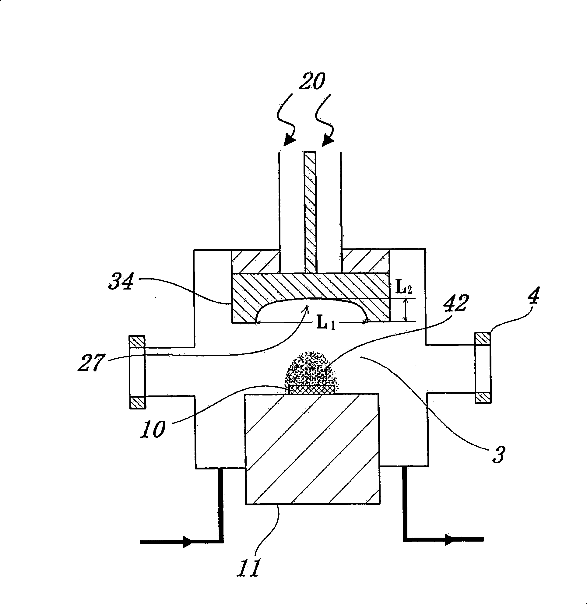
[0069] use as figure 2 The electrode portion 34 shown comprising an oblate spherical recess 27 replaces as figure 1 The antenna part 25 of the microwave plasma CVD apparatus is shown. For the size of the recess 27, the diameter at the surface facing the center of the vacuum chamber (L 1 ) is made equal to the length of 1 wavelength and will be the depth from the surface facing the center of the vacuum chamber to the deepest part of the recess (L 2 ) is made equal to 1 / 5 wavelength. As the substrate 10, a 2×2×0.3 mmt high temperature and high pressure synthetic IIa(111) single crystal substrate placed in the center in a square shape and a As the base material of the molybdenum disk, the same experiment as in Example 1 was carried out. The power of the microwave 20 was 3 kW to generate the plasma 42 , and when the upper and lower positions of the substrate support table 11 were adjusted, the single crystal substrates of all five configurations were covered with the hemisph...


PUM


Abstract

A microwave plasma CVD system in which positional control of plasma can be carried out satisfactorily under such conditions as a large area high quality diamond thin film can be deposited. The microwave plasma CVD system comprises a vacuum chamber (1) having an aperture (2) in the upper center for introducing microwave (20); a substrate supporting base (11) for supporting a substrate in the vacuum chamber; a waveguide for guiding a microwave to the aperture; a dielectric window (22) for introducing a microwave into the vacuum chamber; and an antenna section (25), which is arranged for introducing a microwave into the vacuum chamber, and is composed of a round rod portion (23) located in the center of the waveguide, the aperture and the dielectric window, and an electrode portion (24) combined with the upper portion of the vacuum chamber to clamp the dielectric window for the purpose of holding vacuum. The end face of the electrode portion (24) is formed wider than the dielectric window to conceal the dielectric window, and a recess (26) of a predetermined size is formed on the surface of the electrode portion (24) on the center side of the vacuum chamber.

Description

technical field [0001] The present invention relates to a microwave plasma CVD apparatus for forming carbon films such as diamond films, diamond-like carbon films and carbon nanotubes and films such as silicon oxide films, silicon nitride films and non- For silicon thin films such as crystalline silicon thin films, the microwave plasma CVD apparatus is especially used for forming diamond thin films. Background technique [0002] Chemical vapor deposition (CVD) is widely used for the formation of carbon thin films, especially diamond thin films. Using, for example, methane and hydrogen as raw materials, radicals as diamond precursors are formed by raw material gas activation equipment such as microwaves, hot wires, high-frequency or DC discharges, and diamonds are deposited on substrates. [0003] Since diamonds have the highest hardness among naturally occurring materials, they are used for cutting tools and the like, and they also have very excellent physical properties as...

Claims


Application Information

Patent Timeline
Patent Type & Authority Applications(China)
IPC IPC(8): C23C16/511C30B29/04H01L21/205
CPCC30B25/105C23C16/24C23C16/511C30B29/04H01J37/32192H01J37/32238
Inventor 植田晓彦目黑贵一山本喜之西林良树今井贵浩
Owner SUMITOMO ELECTRIC IND LTD
Why Eureka
Try Eureka