Method and system for fabrication of integrated tunable/switchable passive microwave and millimeter wave modules

a technology of switchable passive microwave and millimeter wave module, which is applied in the direction of waveguides, microstructural technology, coils, etc., can solve the problems of low rf performance, low q resonator, and low q capacitors, etc., and achieves low cost and high q components. , the effect of limiting the rf and microwave application

Inactive Publication Date: 2005-04-05
INTERUNIVERSITAIR MICRO ELECTRONICS CENT (IMEC VZW)
View PDF8 Cites 241 Cited by
  • Summary
  • Abstract
  • Description
  • Claims
  • Application Information

AI Technical Summary

Problems solved by technology

However today a situation has been reached where the presence of the expensive, off-chip passive RF components, whether tunable or not, such as high-Q capacitors, high-Q inductors, resistors, switches, varactor diodes, high-Q resonators, and filters plays a limiting role.
The latter based technologies, i.e. PCB or PWB based technologies are most commonly used in low frequency digital applications, and are not very suited for RF and microwave applications.
However, despite many years of research, such on-chip passive components based on electronic solutions, implemented and / or integrated in various RF-IC (Radio Frequency integrated circuit) technologies including BiCMOS, SiGe and GaAs, did not result in components with the high-quality offered by discrete passive components and which are required by most wireless applications.
Further, the on-chip passive components based on RF-IC technologies (BiCMOS, SiGe or GaAs) do not offer the high-quality as required by most wireless applications e.g. the Q-factor of the inductors is typically below 10, whereas Q-factors exceeding 30 are desired.
One reason for the worse RF-behaviour is the lossy substrates used in standard processes.
Even in case of high quality substrates the RF-performance can be low.
Due to the limited dimensions of the conductor wiring interconnecting the active and fixed passive devices on the substrate dielectric losses can be high.
Not only the RF-performance but also the technology cost is an important issue.
Development of passive devices in such technology is however expensive as such changes might affect the overall technology, including the active devices.
The development of a monolithic process is a complex and time-consuming process.
As elucidated earlier however, the RFIC technologies are not suited for fabricating high quality IPDs, which limits the field of application of these technologies.
Such processing has the disadvantage that a MEMS device consumes relatively large and thus expensive chip area.
Further the process freedom of such monolithic integrated IPD is limited.
Such process restriction will limit the type and number of IPD feasible in this monolithic approach.
Although the RF-MEMS technology has clear advantages as explained above, the technology also displays drawbacks.
For instance, the interconnection levels are very limited and so are the number and quality of fixed passives.
Hence, it can be said, that none of the aforementioned technology platforms offers a flexible, cost-effective solution for the fabrication of a wide range of fixed or tuneable high quality RF and microwave IPDs.

Method used


Image

  • Method and system for fabrication of integrated tunable/switchable passive microwave and millimeter wave modules
  • Method and system for fabrication of integrated tunable/switchable passive microwave and millimeter wave modules
  • Method and system for fabrication of integrated tunable/switchable passive microwave and millimeter wave modules

Examples


Embodiment Construction

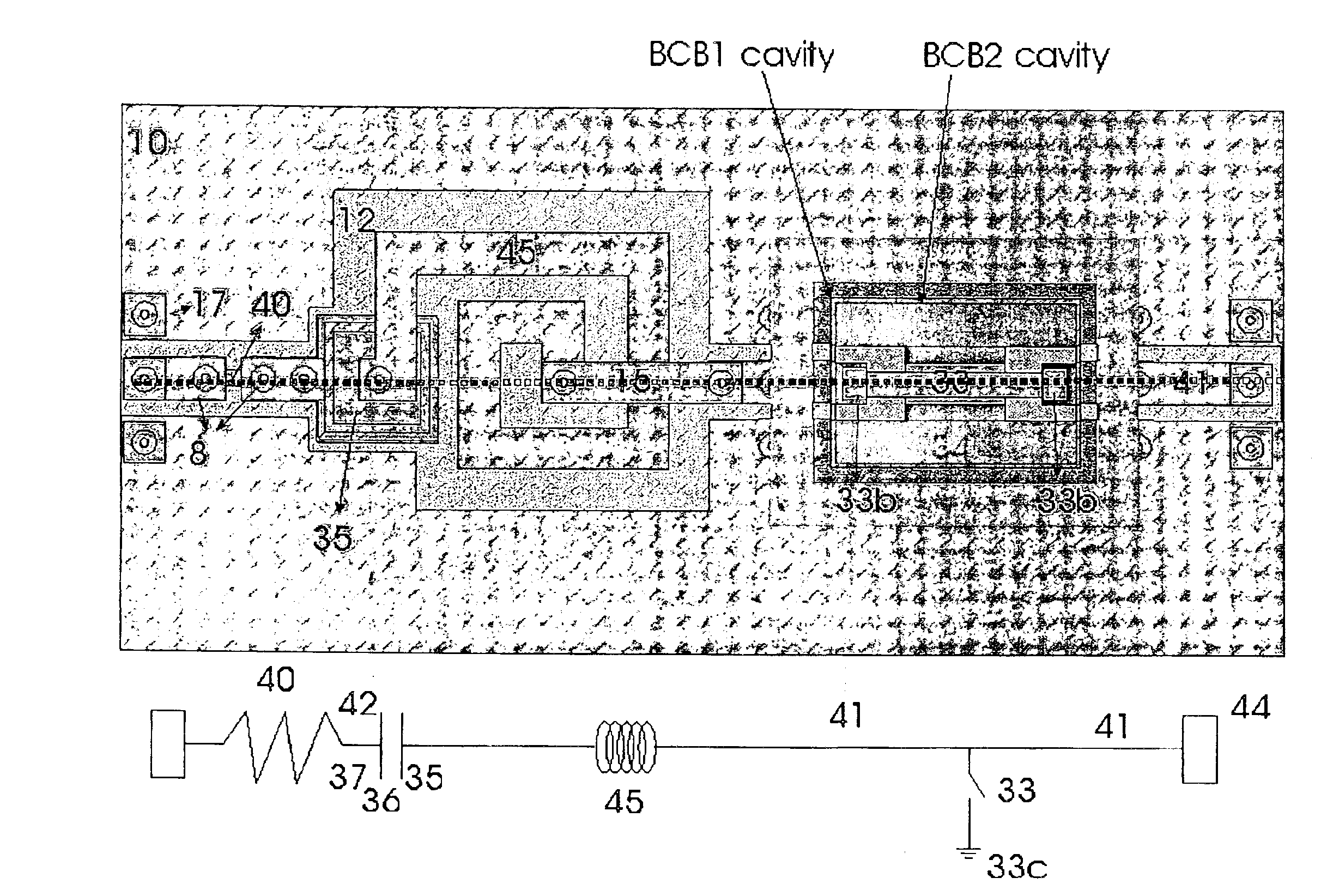
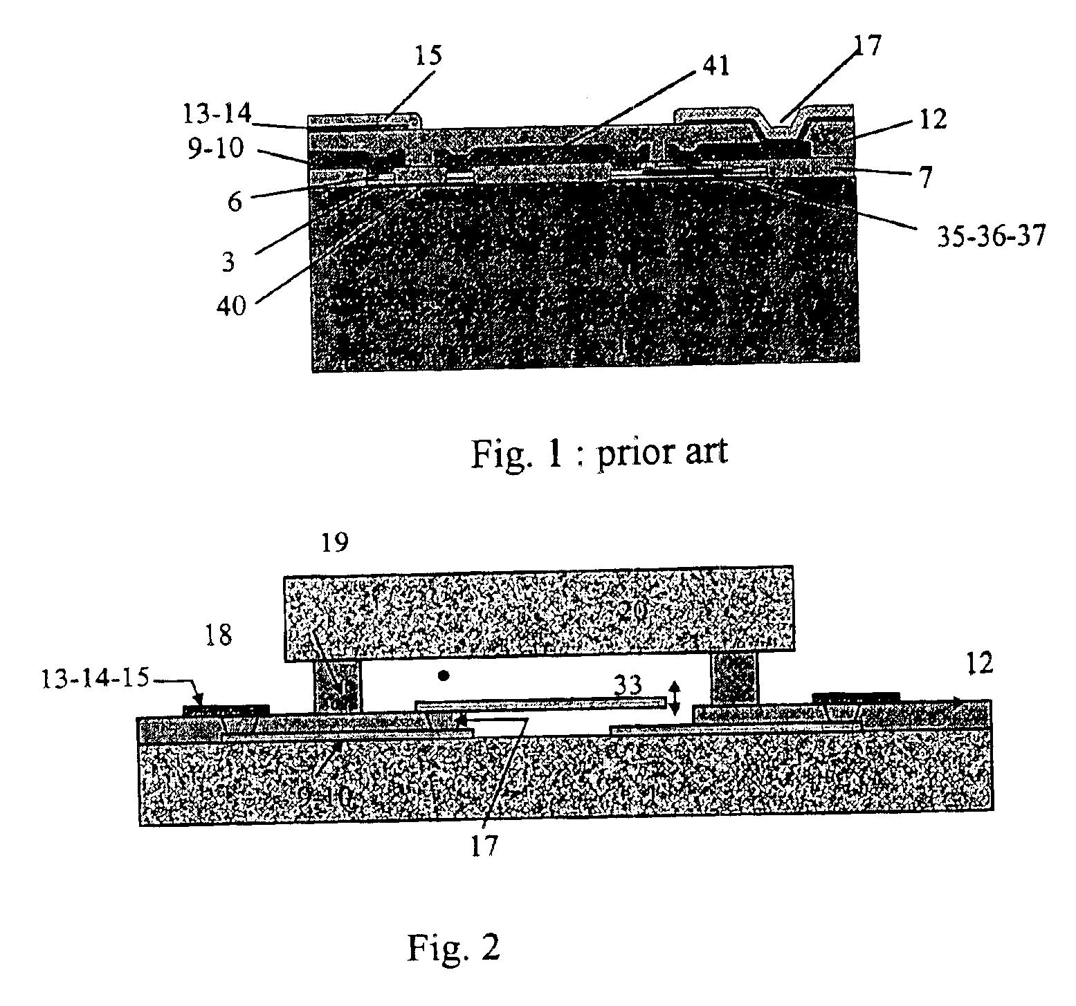
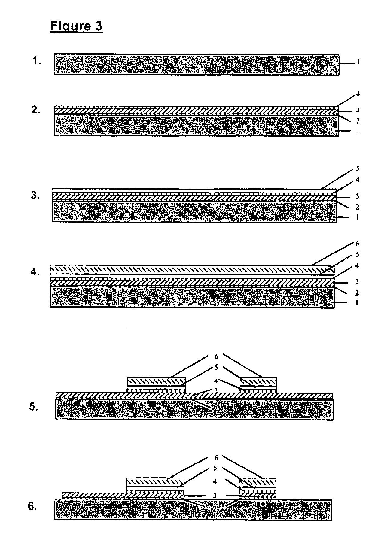
The present invention will be described with reference to certain preferred embodiments and drawings but the present invention is not limited thereto but only by the claims. In particular in the following the material BCB will be described for use as the interlevel dielectric material. Other materials may be used as known for instance from the book by Doane and Franzon mentioned above.

The concept of integration of passive components is to combine various passive elements onto one substrate, thereby creating added value in terms of cost, miniaturisation, reliability, functionality and performance. The present invention provides a platform capable of simultaneous forming and / or integrating a large number of fixed and variable passive devices, whereby a variable device has at least one moveable component or element. Preferably this platform also provides the integration of active devices in a flexible, easy and adaptable way. The combination of active devices and of passive devices is ...


PUM


Abstract

An interconnect module and a method of manufacturing the same is described comprising: a substrate, an interconnect section formed on the substrate, and a variable passive device section formed on the substrate located laterally adjacent to the interconnect section. The interconnect section has at least two metal interconnect layers separated by a dielectric layer and the variable passive device has at least one moveable element. The moveable element is formed from a metal layer which is formed from the same material and at the same time as one of the two interconnect layers. The moveable element is formed on the dielectric layer and is released by local removal of the dielectric layer. Additional interconnect layers and intermediate dielectric layers may be added.

Description

FIELD OF THE INVENTIONThe present invention relates to the fabrication of integrated tunable and / or switchable passive microwave and millimeter wave modules with interconnects to other devices.BACKGROUND OF THE INVENTIONThere has been an explosive growth in wireless communication and the emergence of commercial and consumer applications of radio frequency (RF), microwave, and millimeter-wave circuits and systems in a number of areas. These areas include wireless personal communication and local area networks (WLAN), satellite communications, and automotive electronics. Future personal and ground communications systems as well as communications satellites impose requirements such as very low weight and low power consumption, and small volume. The decrease in size and weight, the ever increasing frequency as well as the trend toward greater functionality of the communications systems, platforms are necessitating the use of highly integrated RF front-end circuits. Continuing chip scali...

Claims


Application Information

Patent Timeline
Patent Type & Authority Patents(United States)
IPC IPC(8): H01L21/70H01L27/12H01L21/84H01P1/10H01P1/12H01H59/00
CPCB81B7/0006H01P1/127H01L27/12H01L21/84H01H59/0009
Inventor TILMANS, HENDRIKUSBEYNE, ERICJANSEN, HENRIDE RAEDT, WALTER
Owner INTERUNIVERSITAIR MICRO ELECTRONICS CENT (IMEC VZW)
Why Eureka
Try Eureka