Chip type balance-unbalance transformer

A balanced transformer and balanced technology, applied in transformers, fixed transformers, transformers/inductor coils/windings/connections, etc., can solve the problem that the winding turns ratio cannot be improved, the impedance conversion ratio is enlarged, and the wiring space is large. Energy conversion loss And other issues

Active Publication Date: 2009-04-22
REALTEK SEMICON CORP
View PDF0 Cites 25 Cited by
  • Summary
  • Abstract
  • Description
  • Claims
  • Application Information

AI Technical Summary

Problems solved by technology

There are also windings formed on the same layer to increase the coupling coefficient, but limited by the limited wiring area, the winding turns ratio cannot be improved
In addition, due to the limitations of the characteristics of the semiconductor process, the uppermost circuit can withstand a higher current density than the other layers of the circuit. Therefore, if there is an interruption in the winding and it needs to be connected by a metal bridge, the entire circuit can carry The current will be limited by the current density that other layers can withstand, and it will not be able to meet the needs of high and low impedance conversion
Especially in the field of power conversion, failure to increase the impedance conversion ratio means that more conversion stages are required, which means more wiring space and greater energy conversion loss

Method used


Image

  • Chip type balance-unbalance transformer
  • Chip type balance-unbalance transformer
  • Chip type balance-unbalance transformer

Examples


Embodiment Construction

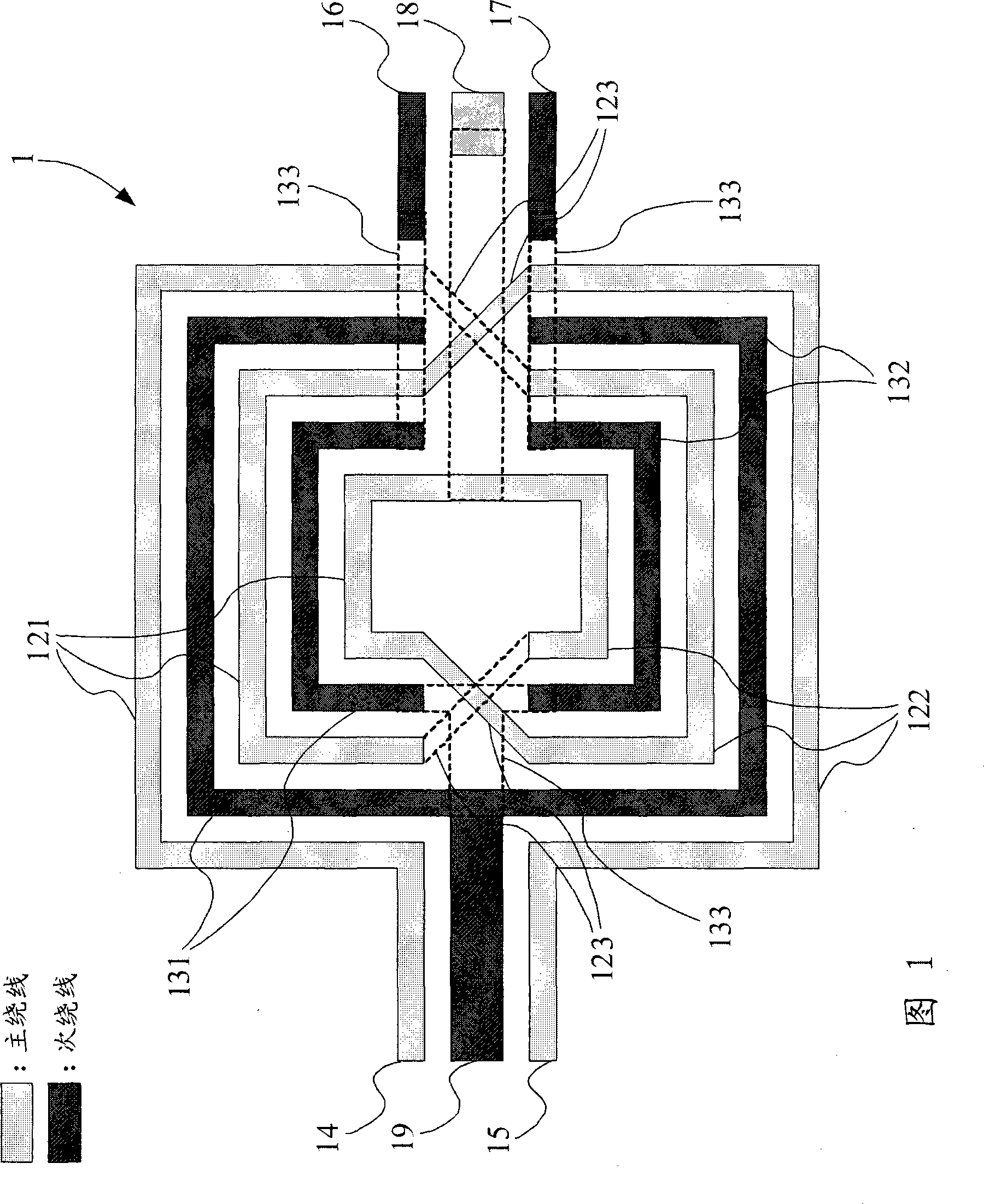
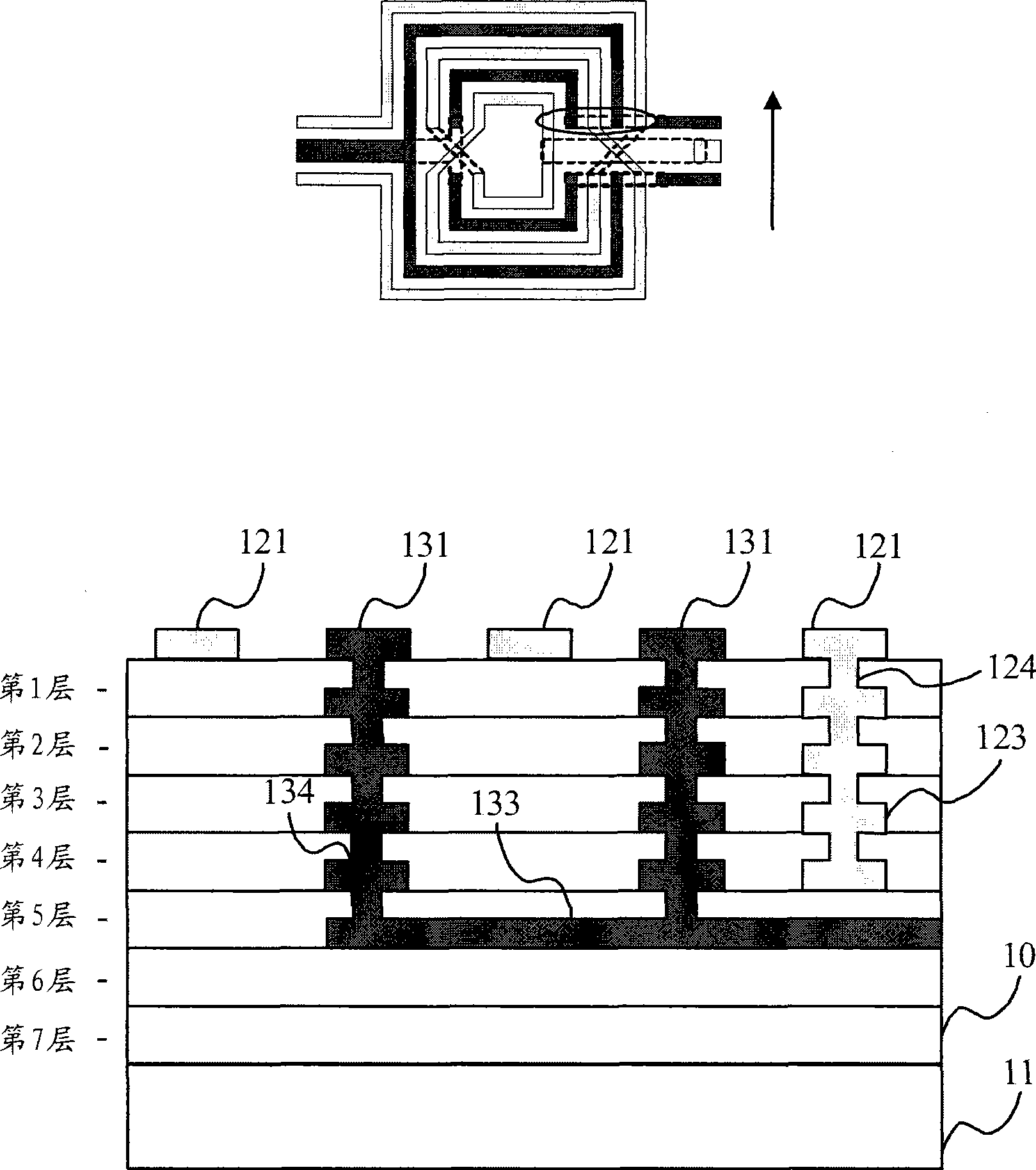
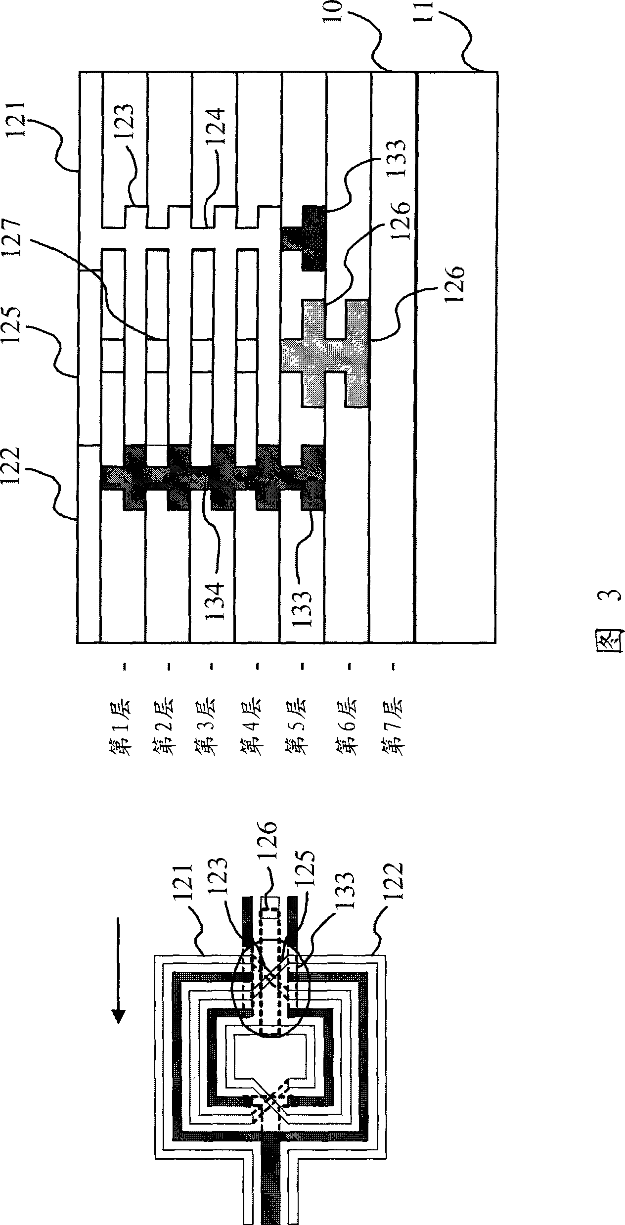
[0028] Please refer to FIGS. 1 to 4 together. FIG. 1 is a front view of a chip-type balun according to a preferred embodiment of the present invention. figure 2 is the first partial side view shown in FIG. 1 . figure 2 Contains a thumbnail of Figure 1 as well as this first partial side view. The first partial side view is a side view of the circled part in the thumbnail along the direction of the arrow in the thumbnail. FIG. 3 is a second partial side view of FIG. 1 . Likewise, FIG. 3 contains the miniature view of FIG. 1 and the second partial side view. The second partial side view is a side view of the circled part in the thumbnail along the direction of the arrow in the thumbnail. FIG. 4 is a third partial side view of FIG. 1 . Likewise, FIG. 4 contains the miniature view of FIG. 1 and the third partial side view. The third partial side view is a side view of the circled part in the thumbnail along the direction of the arrow in the thumbnail. It should be noted that ...


PUM


Abstract

The invention discloses a chip-typed balun transformer which is formed in N layers of continuous isolation layers. The transformer comprises a main winding and a secondary winding. The main winding comprises a plurality of first half coils, a plurality of second half coils, a plurality of metal junctions and a plurality of first metal bridges. The secondary winding comprises a plurality of third half coils, a plurality of fourth half coils and a plurality of second metal bridges. The first half coils and the second half coils are connected by the metal junctions and the first metal bridges. The third half coils and the fourth half coils are connected by the second metal bridges. The transformer allows the input current which is greater than the traditional chip type transformer by using the multi-layer first metal bridges.

Description

technical field [0001] The present invention relates to an On-chip transformer balun, and in particular, to a balun capable of withstanding a larger current than a conventional transformer. Background technique [0002] For the existing chip-type balun transformer, the winding methods are in different layers, but there will be obvious parasitic effect problems, and if the turn ratio is high, the coupling coefficient will be reduced. There are also windings formed on the same layer to increase the coupling coefficient, but limited by the limited wiring area, the winding turns ratio cannot be increased. In addition, due to the limitation of the characteristics of the semiconductor process, the uppermost circuit can withstand a higher current density than the other layers of the circuit. Therefore, if there is an interruption in the winding and needs to be connected by a metal bridge, the entire circuit can carry The current will be limited by the current density that other la...

Claims


Application Information

Patent Timeline
Patent Type & Authority Applications(China)
IPC IPC(8): H01F30/06H01F27/28
Inventor 邱珮如
Owner REALTEK SEMICON CORP
Why Eureka
Try Eureka