Imaging device, control method thereof and CMOS image sensor

一种成像设备、控制方法的技术,应用在图像通信、电视、彩色电视的零部件等方向,能够解决原始主信号系统不均一性无法消除等问题

Inactive Publication Date: 2009-04-22
SOCIONEXT INC
View PDF2 Cites 2 Cited by
  • Summary
  • Abstract
  • Description
  • Claims
  • Application Information

AI Technical Summary

Problems solved by technology

However, even in this case, the non-uniformity of the original main signal system cannot be eliminated due to the non-uniformity among the devices constituting each pixel

Method used


Image

  • Imaging device, control method thereof and CMOS image sensor
  • Imaging device, control method thereof and CMOS image sensor
  • Imaging device, control method thereof and CMOS image sensor

Examples


Embodiment Construction

[0028] Preferred embodiments of the present invention will be described in detail below with reference to the accompanying drawings.

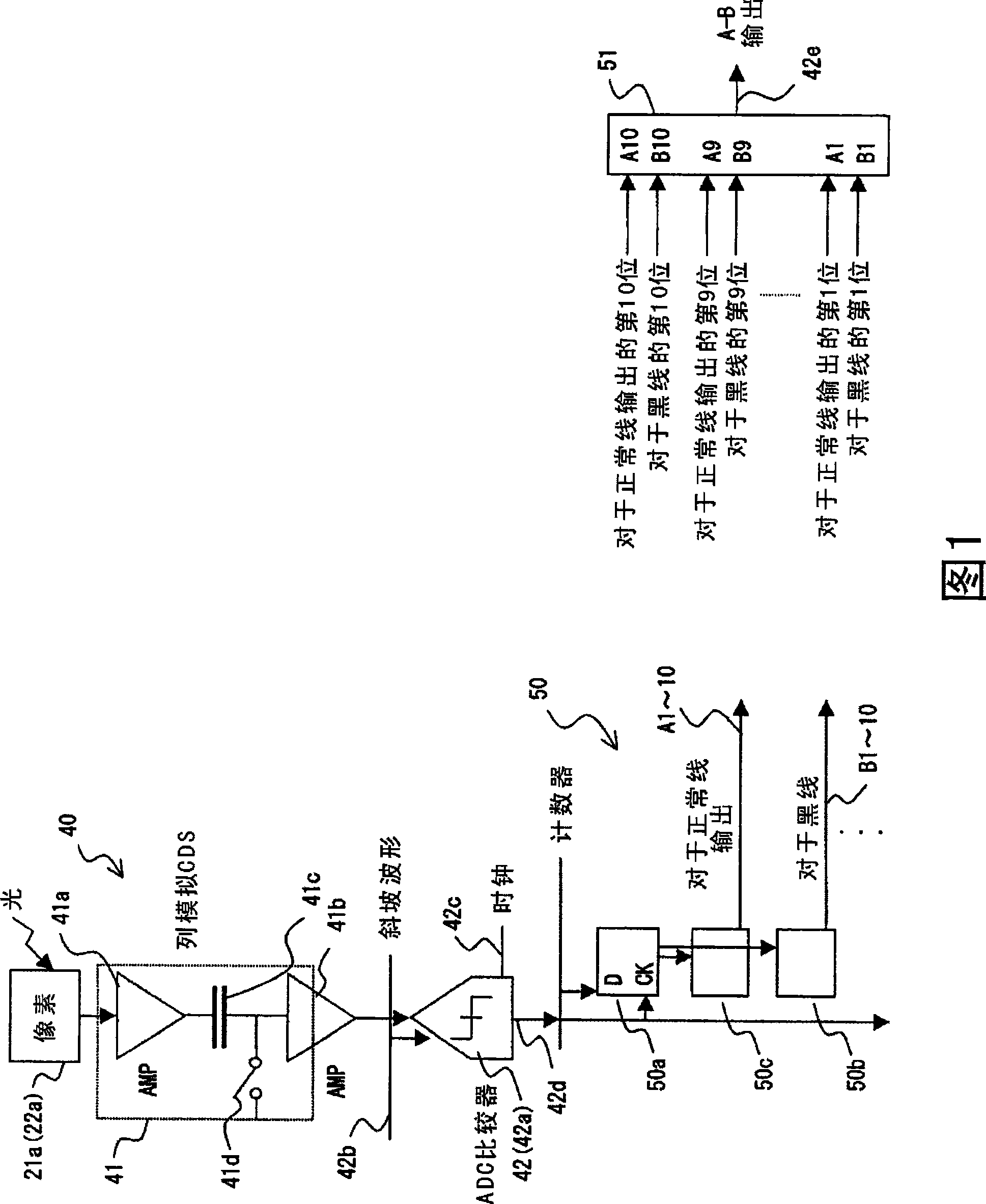
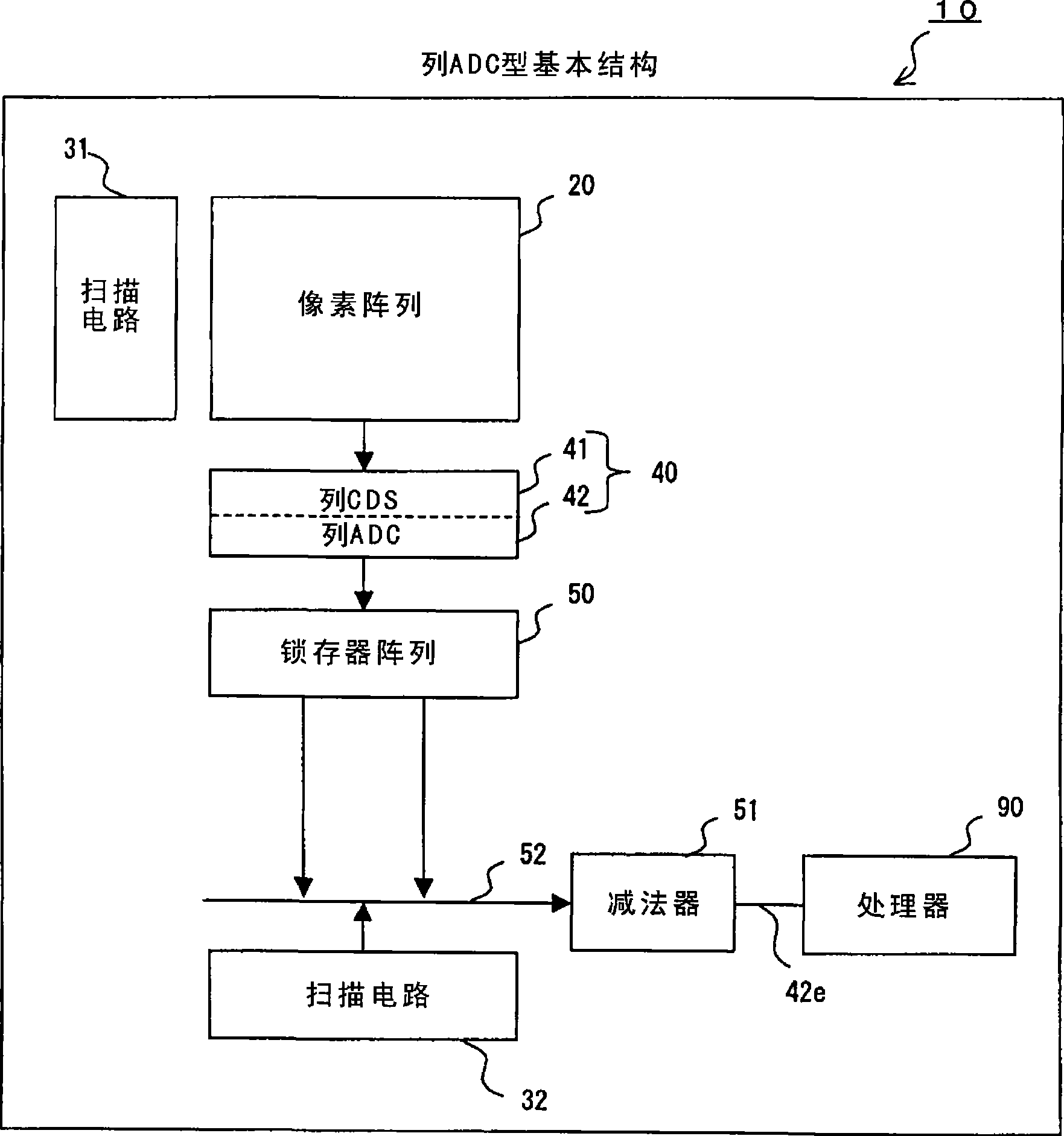
[0029] FIG. 1 is a block diagram showing a part of the structure of an imaging apparatus in a first preferred embodiment of the present invention for realizing a control method. figure 2 An overall structure of the image forming apparatus in the first preferred embodiment of the present invention is conceptually shown. image 3 A part of the image forming apparatus in the first preferred embodiment of the present invention is shown conceptually. 4 and 5 are diagrams showing an example of the functions of the image forming apparatus in each preferred embodiment of the present invention.

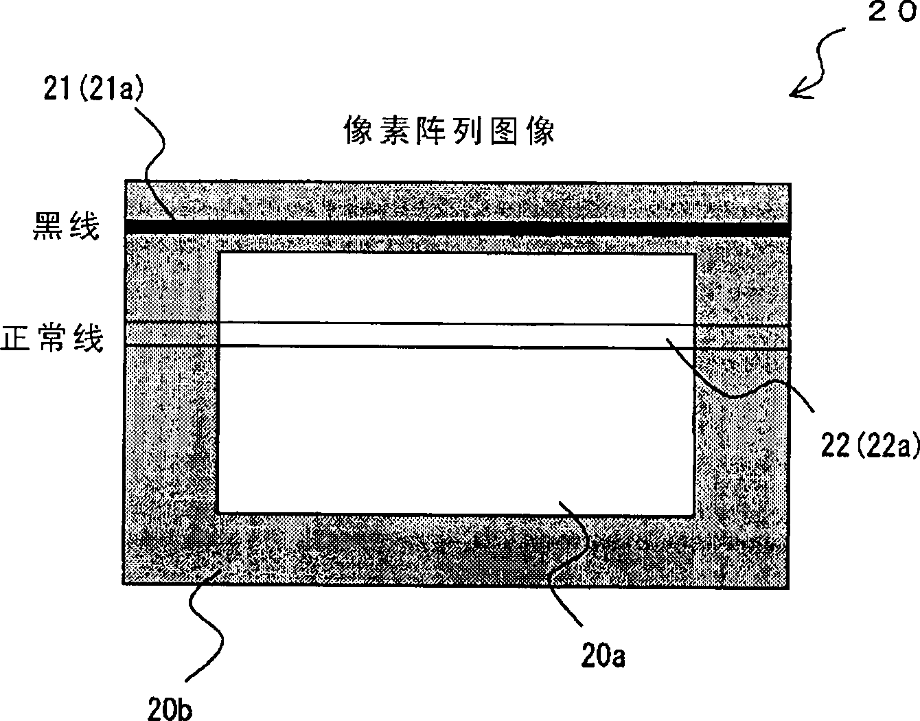
[0030] Such as figure 2 As shown, the imaging device 10 in the first preferred embodiment includes a pixel array 20 of a plurality of pixels each composed of a photo / electric conversion device arranged two-dimensionally in the row and column directions, for r...


PUM


Abstract

The invention provides an imaging device, a control method thereof and a CMOS image sensor. The imaging device provided with a read circuit in which a light-shielding region is formed in a part of an image region where a plurality of optical / electrical conversion devices is two-dimensionally arrayed in the row and column directions and which converts a optically detected signal outputted from each of the optical / electrical conversion devices for each of the column into a digital signal, comprises a storage device for storing the outputted digital signal outputted in relation with the optical / electrical conversion device in the light-shielding region and a difference calculation device for calculating a difference between the outputted digital signal in relation with the optical / electrical conversion device in a light-receiving region except the light-shielding region and a value stored in the storage device.

Description

[0001] This application is a divisional application of Chinese patent application 200510001852.3 filed on January 18, 2005. technical field [0002] The present invention relates to imaging technology, and more particularly, to technology that can be effectively applied to imaging devices such as complementary metal oxide semiconductor (CMOS) image sensors and the like. Background technique [0003] For example, compared with charge-coupled device (CCD) image sensors, CMOS image sensors can be well matched with peripheral image processing circuits in terms of manufacturing process, operating voltage, etc., and in CMOS image sensors, imaging equipment, image processing circuits , controller, etc. can be easily integrated on one chip. [0004] Since in this CMOS image sensor, not only the photo / electric conversion device can be amplified at the level of each pixel, but also the conversion signal can also be amplified at the level of each pixel, so the CMOS image sensor can be ...

Claims


Application Information

Patent Timeline
Patent Type & Authority Applications(China)
IPC IPC(8): H04N5/217H04N5/335H04N5/357H04N5/363H04N5/374H04N5/378
CPCH04N5/378H04N5/3658H04N25/677H04N25/75H04N25/60
Inventor 船越纯山本克义小久保朝生水口寿孝樋口刚
Owner SOCIONEXT INC
Why Eureka
Try Eureka