Silicon on insulator read-write non-volatile memory comprising lateral thyristor and trapping layer

A non-volatile, thyristor technology, used in read-only memory, thyristor, static memory, etc., to solve problems such as affecting applicability

Inactive Publication Date: 2007-06-13
MICRON TECH INC
View PDF4 Cites 0 Cited by
  • Summary
  • Abstract
  • Description
  • Claims
  • Application Information

AI Technical Summary

Problems solved by technology

[0013] Therefore, each of the above units has disadvantages that affect their applicability

Method used


Image

  • Silicon on insulator read-write non-volatile memory comprising lateral thyristor and trapping layer
  • Silicon on insulator read-write non-volatile memory comprising lateral thyristor and trapping layer
  • Silicon on insulator read-write non-volatile memory comprising lateral thyristor and trapping layer

Examples


Embodiment Construction

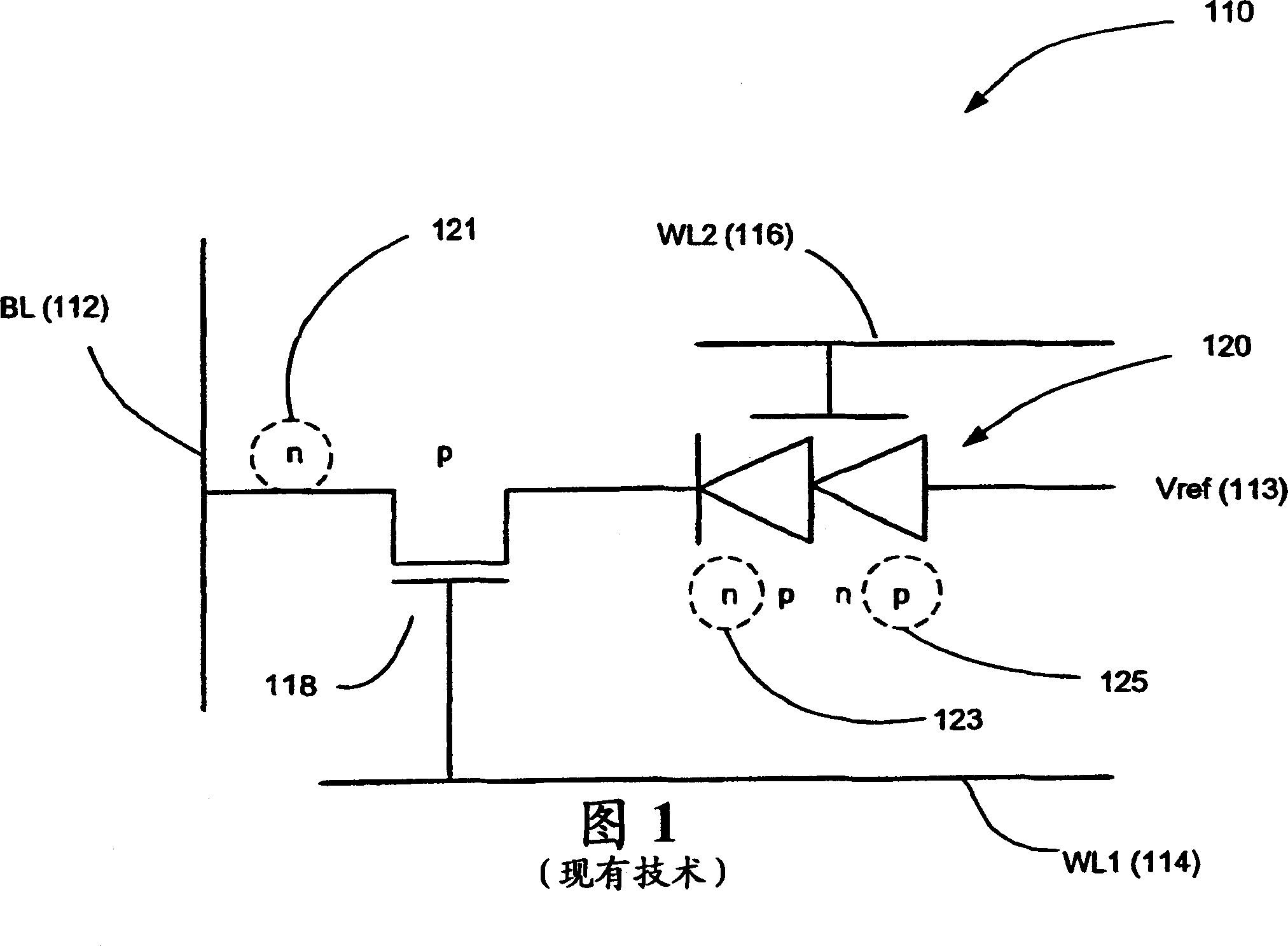
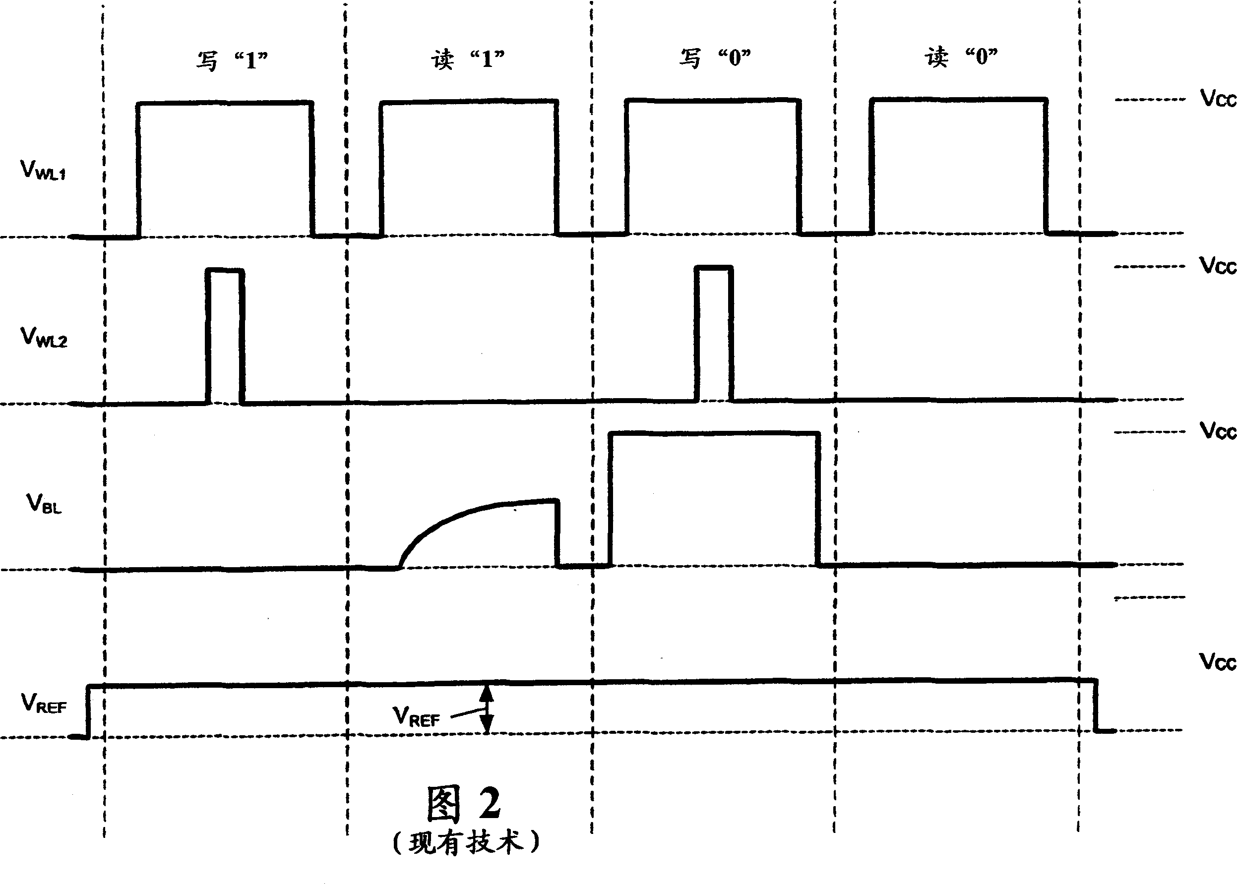
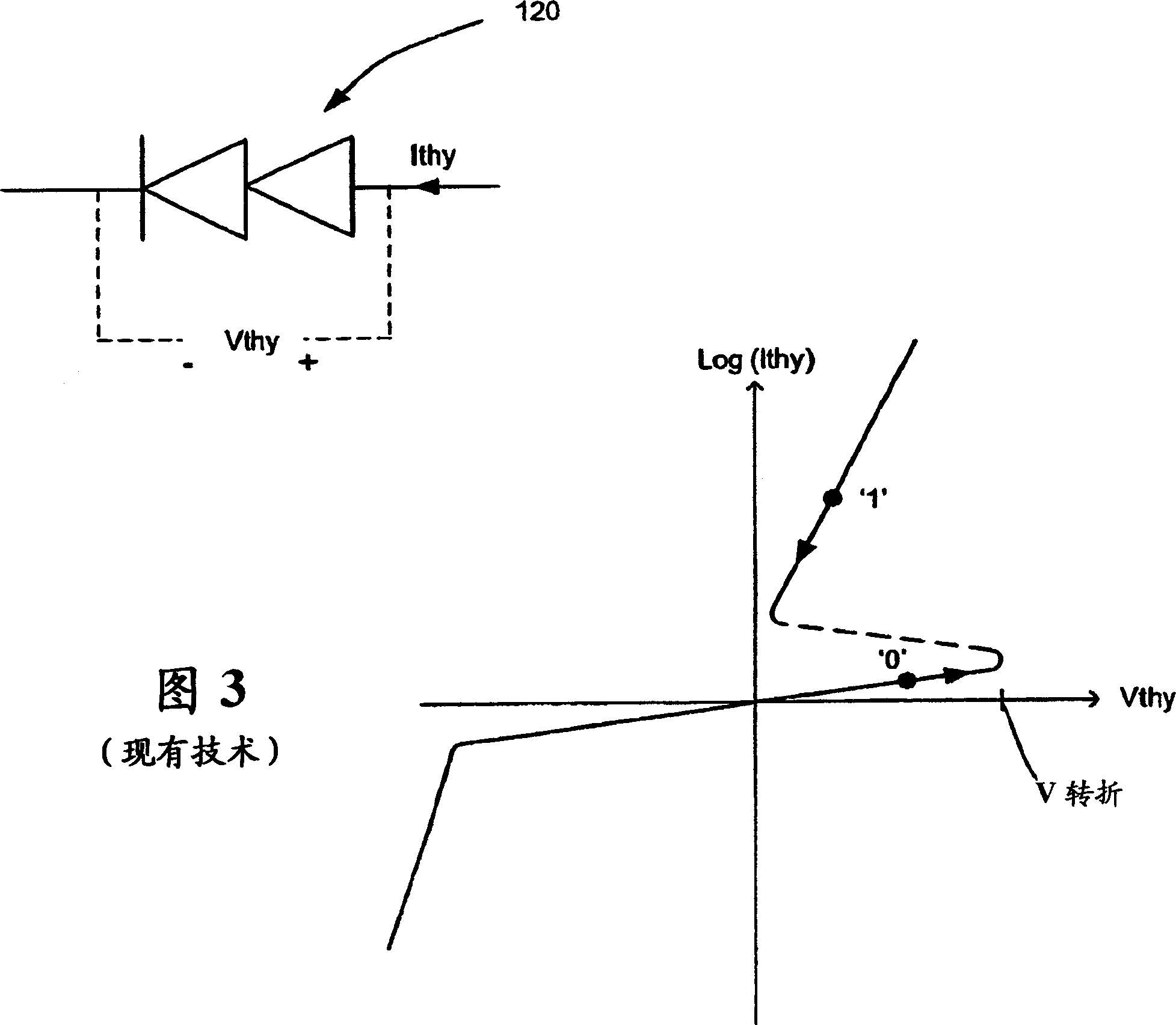
[0025] 4 and 5 show a schematic circuit diagram and a cross-sectional view of an improved thyristor-based cell design 10, respectively. Cell 10 includes elements similar to the thyristor-based cell of FIG. 1 , but differs in several respects. First, the improved cells 10 are preferably, but not necessarily, formed using silicon-on-insulator technology, thereby providing each cell with a floating substrate. As detailed below, this allows the cell to draw lower current and uses the floating body effect to improve the data retention of the cell. Second, the cell design preferably, but not necessarily, incorporates a lateral thyristor formed entirely in the floating silicon substrate. This makes the cell relatively easy to fabricate compared to vertical thyristor-based cells (such as the Nemati reference), or cells that require the thyristor to be at least partially formed on the substrate (such as the '212 application). Also, the insulating floating substrate of each cell prefe...


PUM


Abstract

Disclosed herein is an improved thyristor-based memory cell. In one embodiment, the cell is formed in a floating substrate using Silicon-On-Insulator (SOI) technology. The cell preferably incorporates a lateral thyristor formed entirely in the floating substrate, and which is gated by a second word line. The cathode of the thyristor also comprises a source of an access transistor, whose drain is connected to the bit line of the device, and which is gated by a first word line. A trapping layer is built into the floating substrate, and when writing to the cell, pulses are added to cause holes to be trapped on the trapping layer for a logic state '1' and to cause electrons to be trapped on the trapping layer for a logic state '0'. Trapping of charges on the trapping layer adds extra margin to the stored data states, prevents their degradation, and renders the cell non-volatile.

Description

technical field [0001] The present invention relates to the design of memory cells for integrated circuits. Background technique [0002] There are many different types of memory cell designs in the art, each with its own advantages and disadvantages. For example, a dynamic random access memory (DRAM) cell includes a capacitor and an access transistor. The advantage of this cell design is that it can be made very dense. However, DRAM cells are volatile, meaning that the cells lose their stored data when power is removed from the device. Additionally, DRAM cells, even when powered, must be periodically refreshed to maintain their data state. The advantage of a static random access memory (SRAM) cell is that it can be accessed very quickly. However, SRAM cells draw larger amounts of current and are not very dense since they typically have 4 or 6 transistors in a single cell design. Furthermore, these cells, like DRAM cells, are also volatile. Electrically Erasable Progra...

Claims


Application Information

Patent Timeline
Patent Type & Authority Applications(China)
IPC IPC(8): G11C11/00H01L27/108G11C16/34H01L21/28H01L21/336H01L27/102H01L27/12H01L29/74H01L29/749H01L29/768H01L29/87
CPCH01L29/7436G11C16/349H01L29/66825G11C11/39H01L29/87H01L21/28273H01L27/1027H01L29/749H01L27/1203H01L29/40114
Inventor A·巴塔查里亚
Owner MICRON TECH INC
Why Eureka
Try Eureka