Double patterning strategy for contact hole and trench

A double image and graphics technology, applied in photography, pattern surface photolithography, optics, etc., can solve problems such as unsatisfactory process results, inconvenience, and inappropriateness

Active Publication Date: 2009-06-03
TAIWAN SEMICON MFG CO LTD
View PDF4 Cites 20 Cited by
  • Summary
  • Abstract
  • Description
  • Claims
  • Application Information

AI Technical Summary

Problems solved by technology

For example, in the lithographic patterning process, the photoresist layer is susceptible to pattern collapse and critical dimension reduction, which makes the process results unsatisfactory
[0003] It can be seen that the above-mentioned existing lithography pattern forming method obviously still has inconvenience and defects in method and use, and needs to be

Method used


Image

  • Double patterning strategy for contact hole and trench
  • Double patterning strategy for contact hole and trench
  • Double patterning strategy for contact hole and trench

Examples


Embodiment Construction

[0037] In order to further explain the technical means and effects that the present invention adopts to achieve the intended purpose of the invention, below in conjunction with the accompanying drawings and preferred embodiments, the specific implementation methods, methods, steps, Features and their functions are described in detail below.

[0038] The aforementioned and other technical contents, features and effects of the present invention will be clearly presented in the following detailed description of preferred embodiments with reference to the drawings. Through the description of the specific implementation mode, when the technical means and functions adopted by the present invention to achieve the predetermined purpose can be obtained a deeper and more specific understanding, but the accompanying drawings are only for reference and description, and are not used to explain the present invention be restricted.

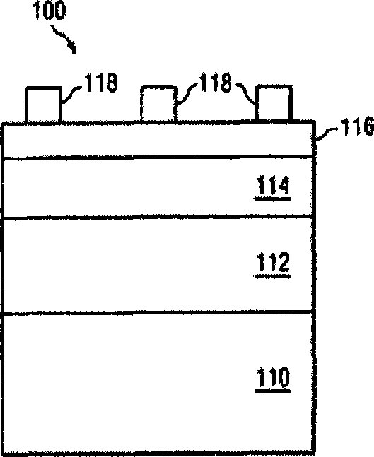
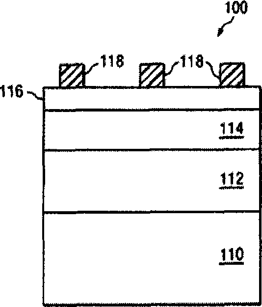
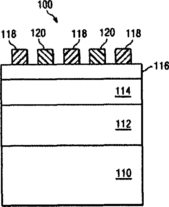
[0039] Figure 1 to Figure 8It is a cross-sectional view ...


PUM


Abstract

A method of lithography double patterning includes forming a first resist pattern on a substrate, the first resist pattern including at least one opening therein on the substrate; curing the first resist pattern; forming a second resist pattern on the substrate; forming a material layer on the substrate; and removing the first and second resist patterns to expose the substrate. Thereby, double resist pattern, that is the first resist pattern and the second resist pattern, is formed by using lithography double patterning, a separated spcacing between the first resist pattern and the second resist pattern results in a reduced minimum features size.

Description

technical field [0001] The invention relates to a lithographic pattern forming method, in particular to a lithographic double pattern forming method. Background technique [0002] Semiconductor technology continues to move toward smaller dimensions in modern times. In recent years, the size has evolved to 65 nanometers, 45 nanometers, and even smaller processes (that is, manufacturing processes, which are referred to as processes herein). The photoresist layer used to create the layout of tiny integrated circuits usually has a high aspect ratio. Under the above circumstances, how to maintain an ideal critical dimension (CD) will be more difficult due to many influencing factors. One of the challenging items is the critical dimension of the photoresist layer. For example, in the lithographic patterning process, the photoresist layer is easily affected by pattern collapse and CD reduction, which makes the process result unsatisfactory. [0003] It can be seen that the abov...

Claims


Application Information

Patent Timeline
IPC IPC(8): G03F7/00G03F7/26G03F7/16H01L21/027
CPCH01L21/76816H01L21/0338H01L21/0337H01L21/31144G03F7/0035
Inventor 许峰诚陈俊光
Owner TAIWAN SEMICON MFG CO LTD
Why Eureka
Try Eureka