Wafer and method for verifying and defect and scanning machine
A defect scanning and wafer technology, applied in the direction of optical testing defects/defects, etc., can solve the problems of difficult frequent use, high cost of standard chips, etc.
- Summary
- Abstract
- Description
- Claims
- Application Information
AI Technical Summary
Problems solved by technology
Method used
Image

Examples
Embodiment Construction
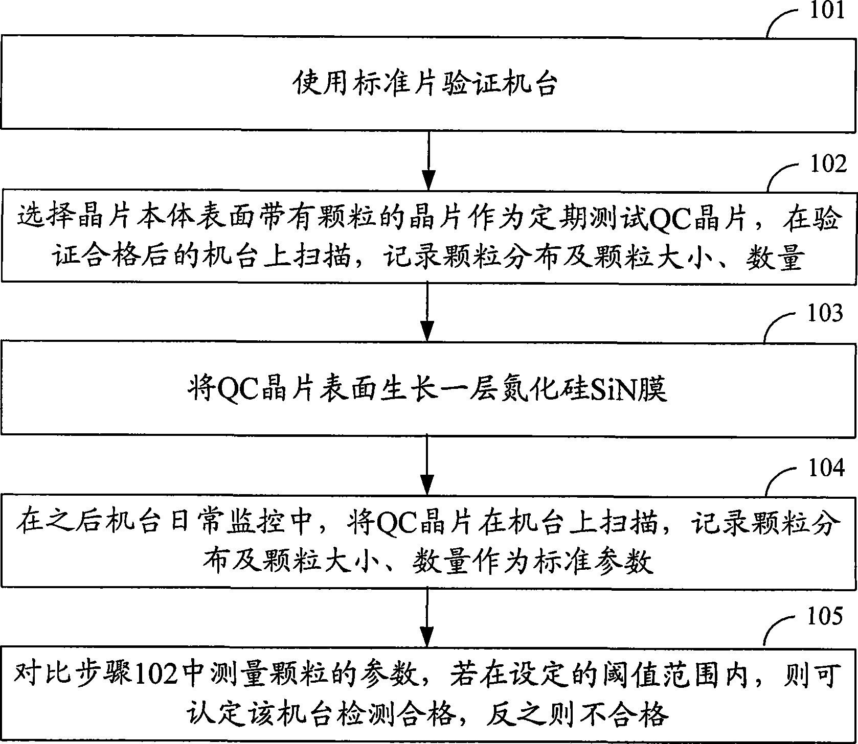
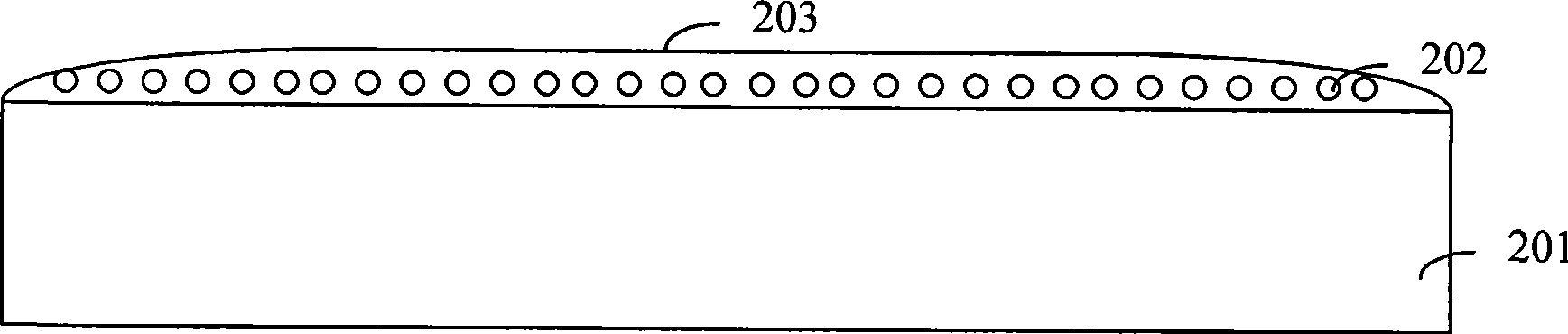
[0012] In order to solve the problem that the cost of standard chips is high and it is not easy to use frequently, the embodiment of the present invention provides a method for verifying defect scanning machines and wafers. The method is to self-made and regularly test QC chips without using standard chips. , to verify the machine. The embodiment of the present invention adopts the following method. Before the test, use a standard chip to verify the accuracy of the machine, and then select a suitable QC chip, scan it on the machine, and record the particle distribution, particle size, and quantity. In order to fix the existing particles of the QC wafer, a layer of SiN film is grown on the surface of the QC wafer, so that the original particles on the surface of the QC wafer are wrapped by the SiN film and will not change with time. The QC wafer covered with SiN film is re-measured on the machine. At this time, the distribution, size and quantity of the particles are the param...
PUM
| Property | Measurement | Unit |
|---|---|---|
| Thickness | aaaaa | aaaaa |
Abstract
Description
Claims
Application Information