Nonvolatile memory device and method for manufacturing the same

A device and nitride film technology, applied in the field of non-volatile memory devices and their manufacturing, can solve the problems such as the inability of Vt to decrease and the limitation of improving the erasing speed, and achieve the effect of improving the erasing speed.

Inactive Publication Date: 2009-07-01
DONGBU HITEK CO LTD
View PDF0 Cites 7 Cited by
  • Summary
  • Abstract
  • Description
  • Claims
  • Application Information

AI Technical Summary

Problems solved by technology

Therefore, in a memory device with a SONONOS or BE-SONOS structure, there may be a limitation in increasing the erasing speed
Additionally, the eras...

Method used


Image

  • Nonvolatile memory device and method for manufacturing the same
  • Nonvolatile memory device and method for manufacturing the same
  • Nonvolatile memory device and method for manufacturing the same

Examples


Embodiment Construction

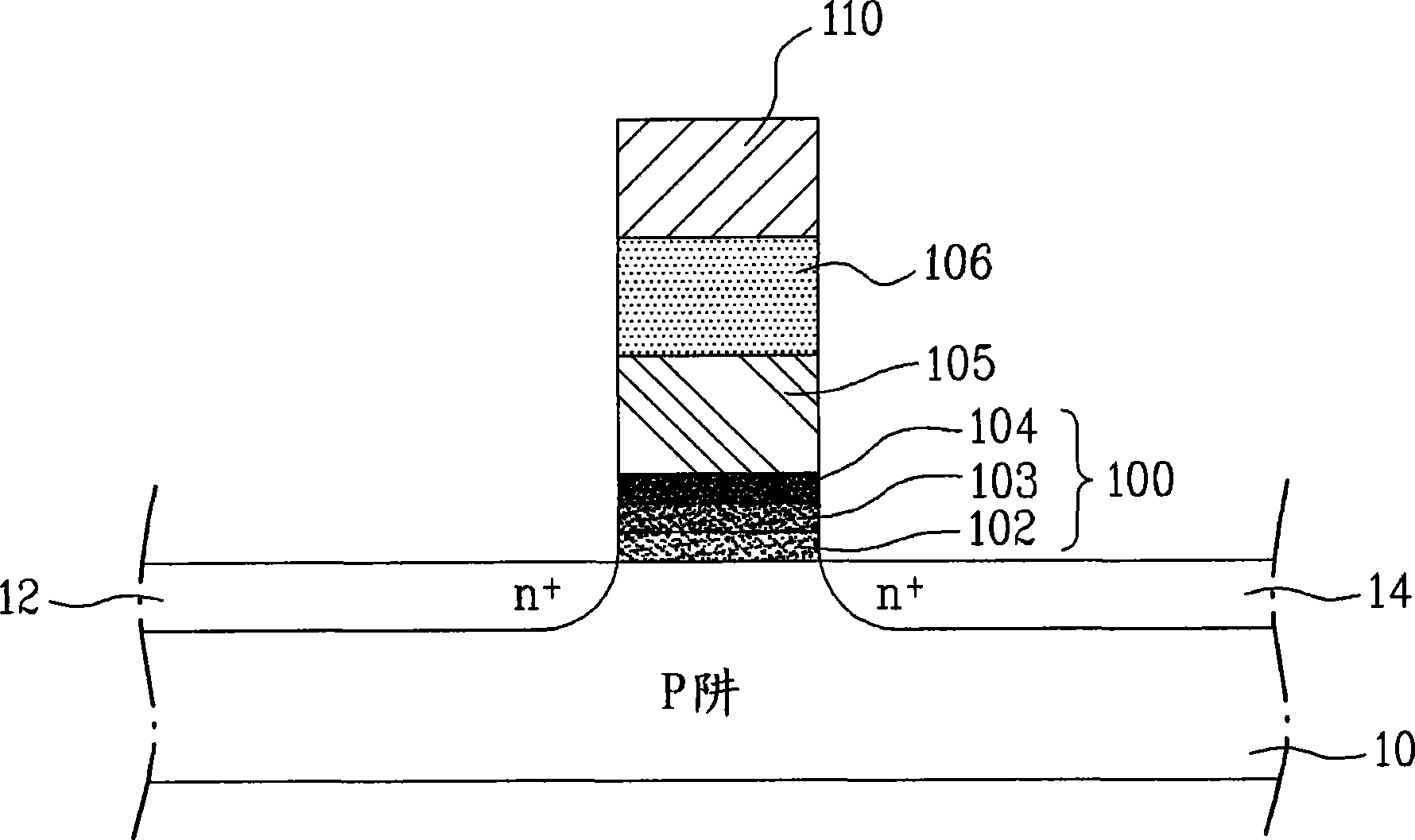
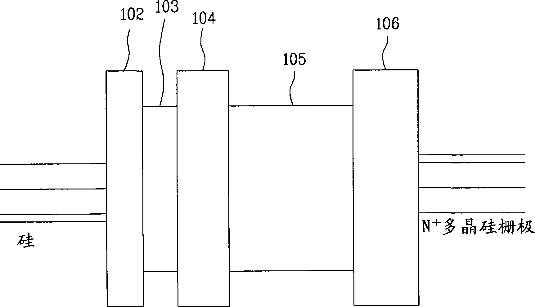
[0022] example Figure 4 is a cross-sectional view showing a nonvolatile memory device according to an embodiment of the present invention. reference example Figure 4 , the nonvolatile memory device 200 may include a tunnel ONO film 210 and a trap nitride film 220 formed on and / or over the tunnel ONO film 210 . The nonvolatile memory device 200 may further include a blocking oxide film 230 formed on and / or over the trap nitride film 220 and a gate 240 formed on and / or over the blocking oxide film 230 . According to embodiments of the present invention, these elements may be sequentially stacked on and / or over semiconductor substrate 202 . According to an embodiment of the present invention, the tunnel ONO film 210 may include an oxide film 212, a nitride film 213, and an oxide film 214, wherein the oxide film 212, the nitride film 213, and the oxide film 214 may be stacked. The device may also include a source 252 and a drain 254 . According to an embodiment of the presen...


PUM


Abstract

Embodiments relate to a nonvolatile memory device and a method for manufacturing the same. According to embodiments, a nonvolatile memory device may include a tunnel ONO film having an oxide film, a nitride film, and an oxide film stacked on and/or over a semiconductor substrate. It may also include a trap nitride film formed on and/or over the tunnel ONO film, a blocking oxide film formed on and/or over the trap nitride film and having a high-dielectric film with a higher dielectric constant than a dielectric constant of a SiO2 film. According to embodiments, a gate may be formed on and/or over the blocking oxide film. An electron back F/N tunneling at the time of an erase operation may be minimized. This may improve an erase speed and erase Vt saturation phenomenon.

Description

[0001] This application claims priority from Korean Patent Application No. 10-2007-0139622 (filed on December 28, 2007) based on 35 U.S.C119, the entire contents of which are hereby incorporated by reference. technical field [0002] The present invention relates to a nonvolatile memory device (nonvolatile memory device) and its manufacturing method, more particularly, to a device with a silicon-oxide-nitride-oxide-nitride-oxide-silicon (SONONOS) structure Or a quantum well nonvolatile memory device with a bandgap engineered (Bandgap Engineered) SONOS (BE-SONOS) structure and a manufacturing method thereof. Background technique [0003] The nonvolatile memory device may be a floating gate based nonvolatile memory device. When adjusting the nonvolatile memory device based on the floating gate to a size of no more than 60nm, due to the cell-to-cell interference effect (interference effect), the cell-to-cell V t The distribution may be relatively large. This may lead to error...

Claims


Application Information

Patent Timeline
IPC IPC(8): H01L29/792H01L29/51H01L21/28H01L21/336
CPCH01L27/11568H10B43/30H01L29/4234H01L29/792
Inventor 郑真孝
Owner DONGBU HITEK CO LTD
Why Eureka
Try Eureka