Boost control chip

A boost control and chip technology, applied in the control/regulation system, adjusting electrical variables, instruments, etc., can solve the problems of reducing the usable space of the circuit and increasing the number of components, so as to increase the usable space, increase the operating voltage, and improve the low effect

Active Publication Date: 2010-08-18
VIA TECH INC
View PDF0 Cites 0 Cited by
  • Summary
  • Abstract
  • Description
  • Claims
  • Application Information

AI Technical Summary

Problems solved by technology

However, the presence of resistor 170 will increase the number of components and reduce the usable space of the circuit

Method used


Image

  • Boost control chip
  • Boost control chip
  • Boost control chip

Examples


Embodiment Construction

[0011] In order to make the features and advantages of the present invention more comprehensible, the preferred embodiments are specifically listed below, together with the accompanying drawings, and are described in detail as follows:

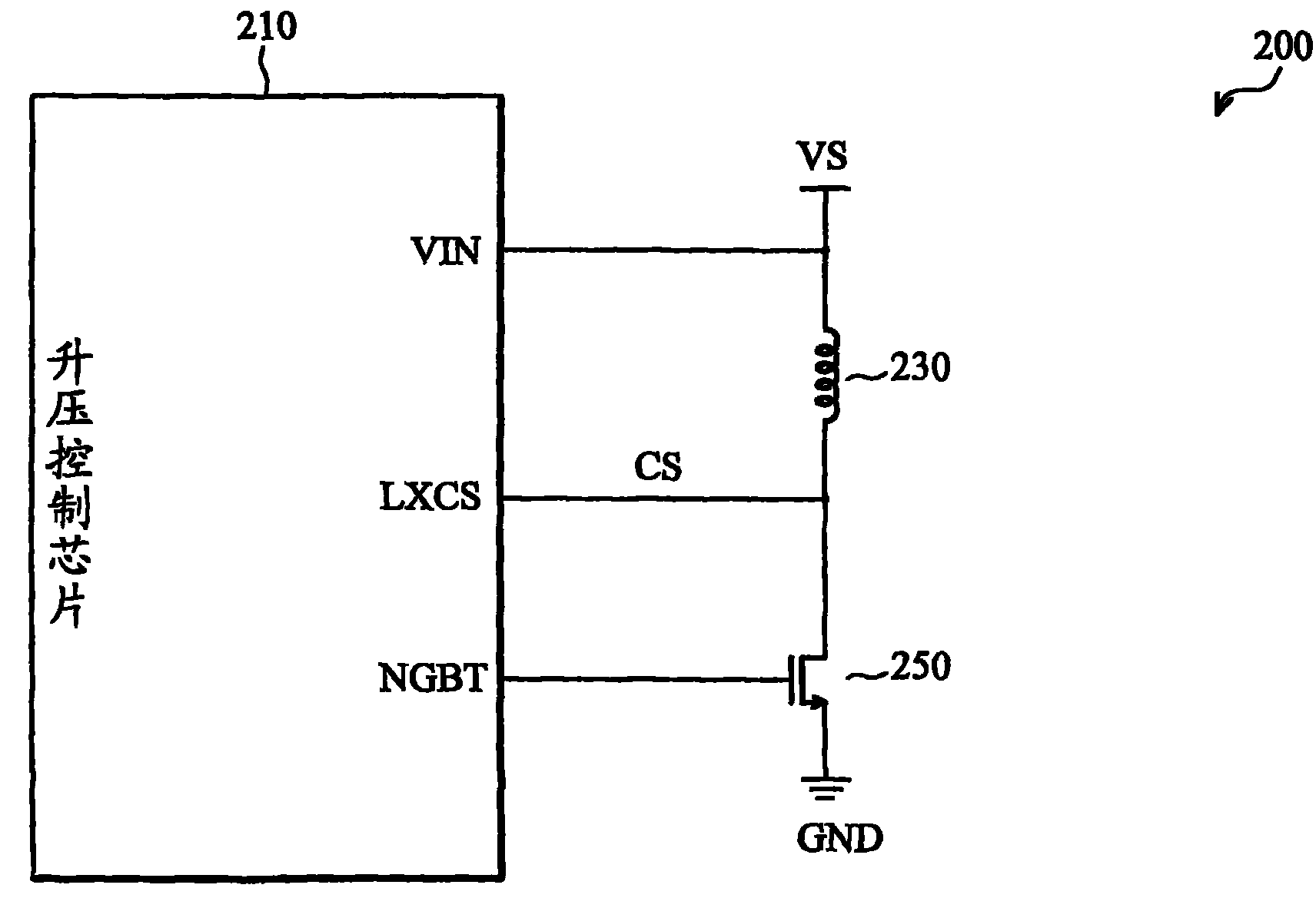
[0012] FIG. 2A is a possible embodiment of the boost circuit of the present invention. In this embodiment, the boost circuit 200 includes a boost control chip 210 , an inductor 230 , and an N-type transistor 250 . The boost control chip 210 has pins VIN, LXCS and NGBT. The inductor 230 is coupled between the pins VIN and LXCS. The gate of the N-type transistor 250 is coupled to the pin NGBT, its source is directly connected to a ground voltage GND, and its drain is coupled to the pin LXCS. The pin VIN of the boost control chip 210 receives the operating voltage VS, wherein the operating voltage VS is greater than the ground voltage GND.

[0013] The boost control chip 210 receives the first voltage CS (that is, the drain voltage of the N-ty...


PUM


Abstract

The invention provides a boost control chip which can be coupled with an inductor and an N-shaped transistor and comprises a first pin, a second pin and a third pin. The first pin is used for receiving an operation voltage and can be coupled with one end of the inductor; the second pin is used for receiving a first voltage and can be coupled with the other end of the inductor and the drain electrode of the N-shaped transistor; the third pin can be coupled with the grid electrode of the N-shaped transistor; and the source electrode of the N-shaped transistor is directly connected with a grounded voltage. The boost control chip provided by the invention can raise the low operation voltage and enhance the application space of circuits.

Description

technical field [0001] The present invention relates to a boost control chip, in particular to a boost control chip applicable to a boost circuit. Background technique [0002] With the advancement of technology, the types and functions of electronic products are increasing day by day, among which portable electronic products are the mainstream in the market. Generally speaking, portable electronic products operate on internal batteries. In order to save the power loss of the battery, the existing practice is to lower the operating voltage of the portable electronic product. However, low operating voltage may not be able to properly drive some components inside electronic products. Therefore, a boost circuit is needed to boost the low operating voltage. [0003] FIG. 1 is a schematic diagram of a conventional boost circuit 100 . In order to know the magnitude of the current flowing through the transistor 150 , the conventional boost circuit 100 has a resistor 170 . The ...

Claims


Application Information

Patent Timeline
Patent Type & Authority Patents(China)
IPC IPC(8): G05F1/10
Inventor 李永胜
Owner VIA TECH INC
Why Eureka
Try Eureka