Reference voltage generating circuit, integrated circuit device, and signal processing apparatus

A reference voltage generation, reference voltage technology, applied in circuits, resistors, electrical components, etc.

Inactive Publication Date: 2009-08-19
SEIKO EPSON CORP
View PDF2 Cites 15 Cited by
  • Summary
  • Abstract
  • Description
  • Claims
  • Application Information

AI Technical Summary

Problems solved by technology

[0017] In this way, in Image 6 The circuit shown has the following problem: only V ref The "vertex temperature deviation" and "output voltage deviation", or V PTAT The “Slope Deviation” and “Output Voltage Deviation” of V ref or V PTAT Changes on either side of the node

Method used


Image

  • Reference voltage generating circuit, integrated circuit device, and signal processing apparatus
  • Reference voltage generating circuit, integrated circuit device, and signal processing apparatus
  • Reference voltage generating circuit, integrated circuit device, and signal processing apparatus

Examples


no. 1 Embodiment approach

[0064] First, an example of a basic circuit configuration will be described.

[0065] (Example of basic circuit configuration)

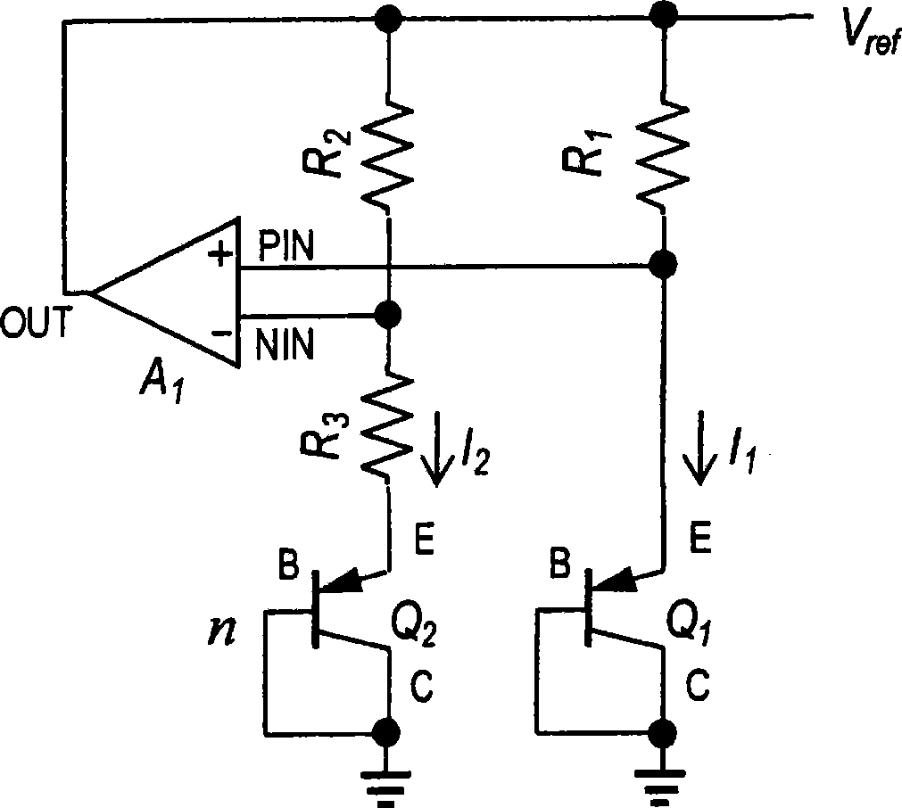
[0066] Figure 7 (A), Figure 7 (B) is a circuit diagram showing an example of the configuration of the reference voltage generation circuit (reference voltage generation circuit with temperature sensor output) of the present invention. The basic circuit structure and Figure 6 The circuit structure is the same. That is, PNP type BJTQ 2 For example, it is configured to connect n in parallel with PNP type BJTQ 1 Same size BJT. In the PNP type BJTQ 1 As a case of BJT, PNP type BJTQ 2 The PN junction area for PNP type BJTQ 1 n times. Let flow through PNP type BJTQ 1 The current is I 1 , flows through a PNP type BJTQ 2 The current is I 2 , for example if I 1 = I 2 , the PNP type BJTQ 2 and Q 1 The current density is 1:n. And, in the following description, the "resistor R 3 "Referred to as the first resistor, the "resistor R 2 "Referr...

no. 2 Embodiment approach

[0117] In this embodiment, another configuration of the variable resistance circuit 500 will be described. Figure 12 (A), Figure 12 (B) is a circuit diagram showing another configuration example of the variable resistance circuit. exist Figure 12 (A), Figure 12 In (B), S0~Sn are terminals for adjustment, but, with Figure 11 (A), Figure 11 (B) differs in the configuration of the bypass switch (the method of inputting the signal indicating the adjustment amount). exist Figure 12 (A), Figure 12 In (B), the bypass switch is respectively connected with the trimming resistor ΔR 30 ~ΔR 3n and trimmed resistor ΔR 40 ~ΔR 4n Correspondingly, when a bypass switch is turned on, the two ends of the corresponding trimming resistor are short-circuited, and only the trimming resistor is invalid.

[0118] exist Figure 11 (A), Figure 11 In (B), it is necessary to set one of the terminals to be H and the remaining terminals to be L. Regarding the adjustment mode, if there...

no. 3 Embodiment approach

[0120] In this embodiment, still another configuration of the variable resistance circuit 500 will be described. Figure 13 (A), Figure 13 (B) is a circuit diagram showing still another configuration example of the variable resistance circuit. exist Figure 13 (A), Figure 13 In (B), S0~Sn are terminals for adjustment, however, in Figure 13 (A), Figure 13 In (B), connect the adjustment resistor (ΔR 30 ~ΔR 3n , ΔR 40 ~ΔR 4n ). And, for each adjustment resistor (ΔR 30 ~ΔR 3n , ΔR 40 ~ΔR 4n ) is provided with switch circuits (MOa~Mna, MOb~Mnb). One end of the switch circuit (MOa~Mna, MOb~Mnb) and each adjustment resistor (ΔR 30 ~ΔR 3n , ΔR 40 ~ΔR 4n ) connection, and the other end is commonly connected. exist Figure 13 In (A), the common connection point of the switching circuits (MOa to Mna) and the second node A 2 connection, the common connection point of the switching circuit (MOb~Mnb) and the fourth node B 2 connect. Only when the switch circuit is ...


PUM


Abstract

The invention provides a benchmark voltage generating circuit, an integrated circuit device and a signal processing device. In the gap circuit of the combined benchmark voltage circuit and a temperature sensor, the invention can inhabit the bias of the benchmark voltage and the version of the bias parties of the output voltages of the temperature sensor. In order to inhibit the top temperature bias and the output voltage bias caused by the inhibition of benchmark voltage (V ref) the elements for adjusting the resistance value of the first resistor (R3), the third resistor (R4) output by the temperature sensor (V PATA) is adjusted by the resistance value. The first resistor (R3) and the third resistor (R4) can be formed by the various circuits for adjusting the resistance value of the various circuits. The device is used for the output of the adjusting signal such as the adjusting circuit (carried on the EEPROM on the IC).

Description

technical field [0001] The present invention relates to a reference voltage generation circuit (especially a reference voltage generation circuit that outputs a temperature-dependent voltage in parallel with a reference voltage), an integrated circuit device, and a signal processing device. Background technique [0002] In integrated circuits (ICs), in the case of processing analog signals, a reference voltage is required. The circuit that generates this voltage is a reference voltage generation circuit. For example, when an analog signal is amplified using an OP amplifier (Operational Amplifier: operational amplifier), amplification may be performed based on a certain reference voltage value. Therefore, when the reference voltage value fluctuates, the analog signal cannot be correctly amplified. A reference voltage is required that always outputs a constant value against fluctuations in the voltage of the power supply supplied to the integrated circuit from the outside an...

Claims


Application Information

Patent Timeline
Patent Type & Authority Applications(China)
IPC IPC(8): G05F3/30H01C10/50
CPCG05F3/30
Inventor 羽田秀生
Owner SEIKO EPSON CORP
Why Eureka
Try Eureka