Test method for asynchronously repairing and adjusting silicon wafer with anti-interference

A wafer testing and trimming technology, applied in electronic circuit testing, semiconductor/solid-state device testing/measurement, etc., which can solve problems such as interference and increase chip interference.

Active Publication Date: 2009-08-19
SINO IC TECH
View PDF0 Cites 18 Cited by
  • Summary
  • Abstract
  • Description
  • Claims
  • Application Information

AI Technical Summary

Problems solved by technology

[0009] At present, in the prior art solution, the fuse probe and the test probe are arranged on the same chip in the above steps, figure 1 It is an enlarged schematic diagram of the corresponding position of the probe 12 on the chip 103 when the existing probe card 10 is used to test the chip 103. Since the fuse probe 122 and the test probe 121 on the probe 12 are simultaneously connected with the fuse on the chip 103 The probe contacts are in contact with the test probe contacts, so that when testing the chip 103, paths are formed between the fuse probes and the fuse probe contacts, between the test probes and the test probe contacts, resulting in fuse Interference problem of the probe on the test of the integrated circuit chip
[0010] In addition, the test environment of the chip during the wafer test is completely different from the use environment after the chip is packaged, which greatly increases the interference of the external environment on the chip during the wafer test

Method used


Image

  • Test method for asynchronously repairing and adjusting silicon wafer with anti-interference
  • Test method for asynchronously repairing and adjusting silicon wafer with anti-interference
  • Test method for asynchronously repairing and adjusting silicon wafer with anti-interference

Examples


Embodiment Construction

[0022] The preferred embodiments of the present invention are given below in conjunction with the accompanying drawings to describe the technical solution of the present invention in detail.

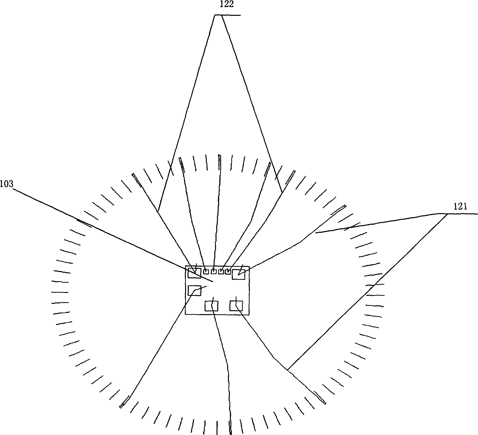
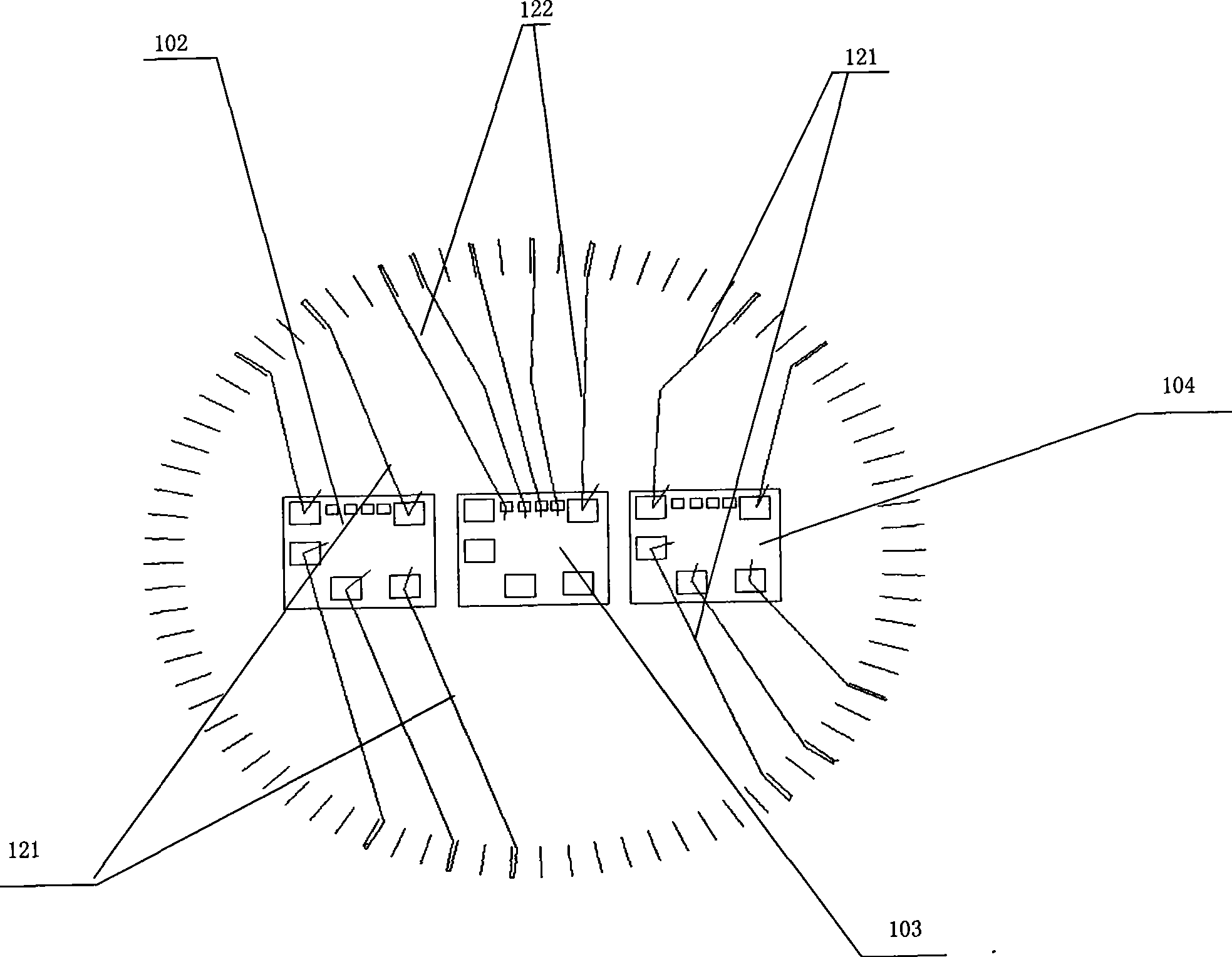
[0023] figure 2 It is an enlarged schematic diagram of the corresponding positions of the fuse probe 122 and the test probe 121 on the adjacent chips 102, 103, 104 on the wafer when the probe card 10 of the present utility model is used for wafer testing. The wire probes are only in contact with the corresponding contacts on the chip 103, and the two groups of test probes are respectively in contact with the test probe contacts on the chip 102 and the chip 104. It can be seen that the fuse probe 122 and the test probe 121 are in the same step. Corresponding to different chips, when testing a certain chip, there will be no interference caused by the fuse probe 122 and the test probe 121 being in contact with the chip at the same time.

[0024] image 3 Shown is the wafer test flow char...


PUM


Abstract

The invention provides a test method of an anti-interference asynchronous trimming wafer, wherein, a probe card is used for testing and trimming a chip on the wafer. Two probes which are a test probe and a fuse probe are arranged on the probe card. The method includes the following steps: step one, the initial value of the chip before a fuse is trimmed is tested; step two, the fuse is trimmed; step three, the final trimming result after the fuse is trimmed is tested. In the three steps, only one probe is adopted to be in contact with the chip for each time. The chip to be tested is only in contact with the test probe and is not in contact with the fuse probe in step one and step three when the relevant parameter values of the chip to be tested are measured, thereby avoiding the interference of the fuse probe in the testing of the chip so as to greatly improve the measuring accuracy of the initial value.

Description

technical field [0001] The invention relates to an anti-interference asynchronous trimming wafer testing method, and in particular to an anti-interference asynchronous trimming wafer testing method in which fuse probes and test probes are respectively arranged on different chips. Background technique [0002] The development of electronic chips includes: chip design, wafer manufacturing, wafer testing, dicing and packaging, packaging and testing, etc. Wafer testing is a test environment built by the test machine and probe card, and the chips on the wafer are tested in this environment to ensure that the electrical characteristics and functions of each chip meet the design specifications and specifications. Chips that fail the test will be marked as bad products and will be screened out in the subsequent dicing and packaging stage. Only chips that pass the test are packaged. Wafer testing is very necessary to reduce the production cost of chips and improve the quality of ch...

Claims


Application Information

Patent Timeline
Patent Type & Authority Applications(China)
IPC IPC(8): H01L21/66G01R31/28
Inventor 张志勇叶守银祁建华岳小兵
Owner SINO IC TECH
Why Eureka
Try Eureka