Supercharge Your Innovation With Domain-Expert AI Agents!

Semiconductor element structure and method for making same

A technology of semiconductor and oxide semiconductor, which is applied in the direction of semiconductor devices, semiconductor/solid-state device manufacturing, semiconductor/solid-state device components, etc. The effect of connection

Active Publication Date: 2011-04-20
UNITED MICROELECTRONICS CORP
View PDF3 Cites 0 Cited by
  • Summary
  • Abstract
  • Description
  • Claims
  • Application Information

AI Technical Summary

Problems solved by technology

However, since the etch back is non-selective with the aid of no mask, the thickness of the electrical connection material is not easy to control and average, and it will also affect the height of the semiconductor element.

Method used


Image

  • Semiconductor element structure and method for making same
  • Semiconductor element structure and method for making same
  • Semiconductor element structure and method for making same

Examples


Embodiment Construction

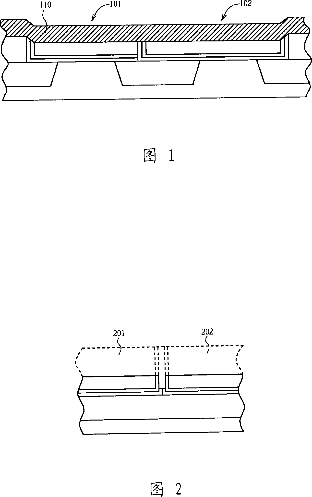
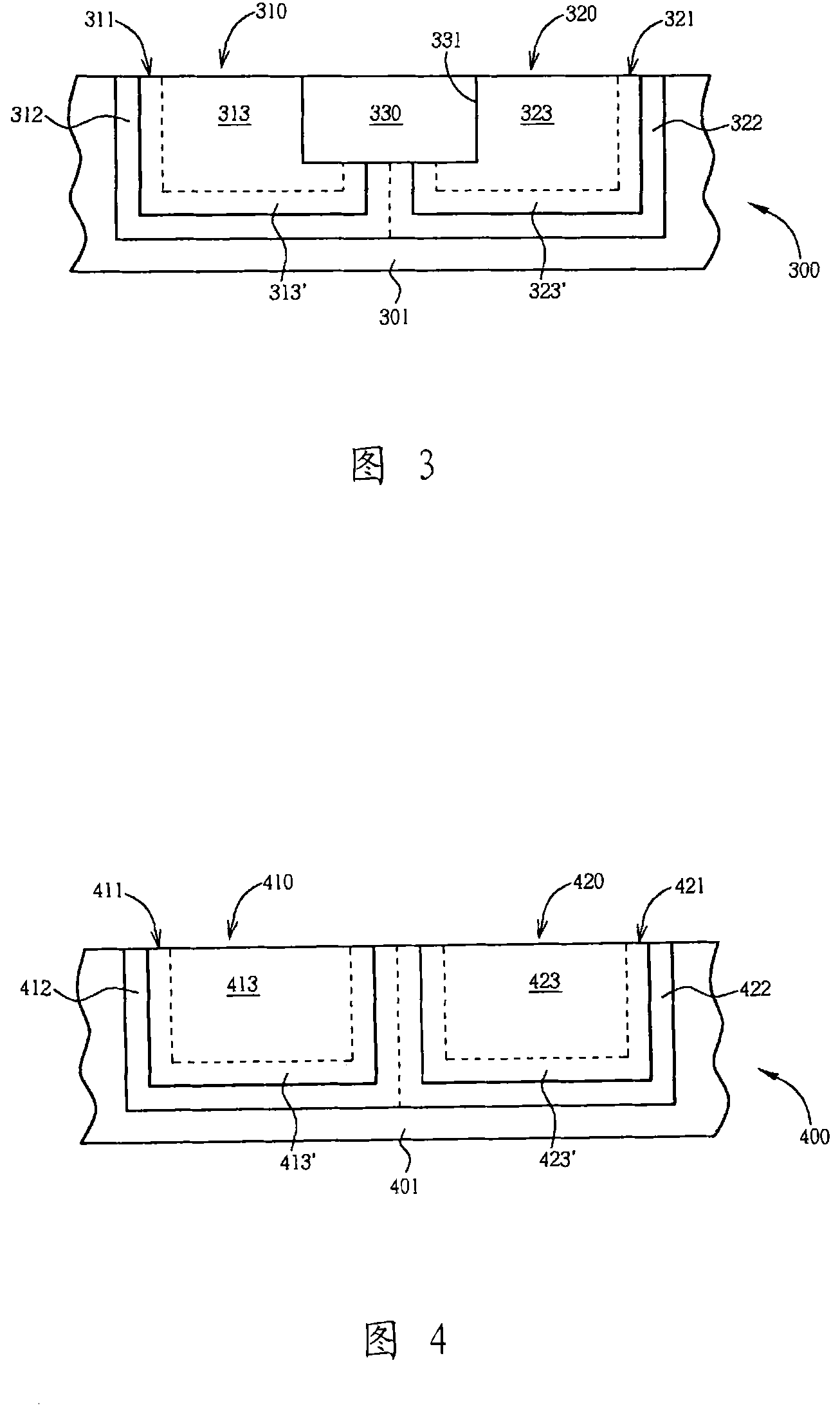
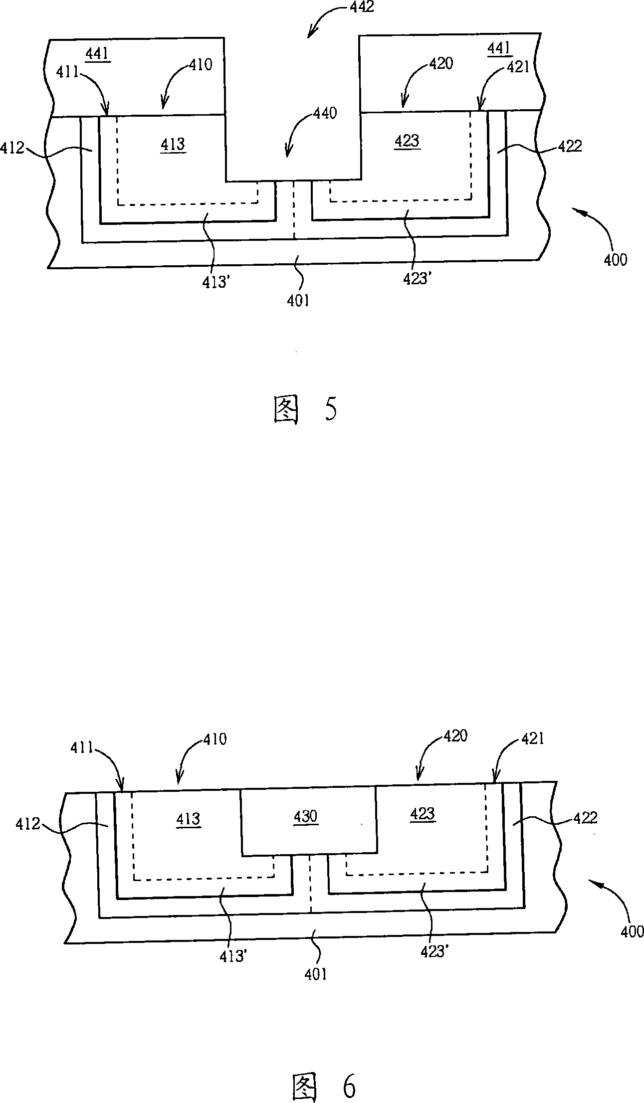
[0033] The present invention is to provide a novel structure of electrical connection between gates, which can be applied in the structures of elements such as inverters and static random access memories (SRAMs), in which the bridge channel will neither The height of the element is not affected, and sufficient and stable electrical connection between the gates can also be ensured.

[0034] Please refer to FIG. 3 , which illustrates a preferred embodiment of the present invention applied to a static random access memory (SRAM) structure. The semiconductor device structure 300 of the present invention includes a substrate 301 , a first metal oxide semiconductor 310 , a second metal oxide semiconductor 320 and a bridging channel 330 . The first metal oxide semiconductor 310 and the second metal oxide semiconductor 320 may respectively represent a P-type metal oxide semiconductor and an N-type metal oxide semiconductor, and include various known components, such as a source (not s...


PUM

PropertyMeasurementUnit
electron work functionaaaaaaaaaa

Abstract

The invention discloses a semiconductor element structure and a method for making the same. The semiconductor element structure comprises: a first metal oxide semiconductor having a first high-dielectric material and a first metal which are used for a first grid; a second metal oxide semiconductor having a second high-dielectric material and a second metal which are used for a second grid and having a bridging channel. The semiconductor element structure is arranged in a groove communicating the first grid and the second grid to connect the first grid and the second grid electrically. The bridging channel is embedded in at least one of the first and second metals.

Description

technical field [0001] The invention relates to a structure of a semiconductor element and a manufacturing method thereof, in particular to a structure of a semiconductor element with bridging channels between gates and a manufacturing method thereof. Background technique [0002] In components such as static random access memory (SRAM) designed with complementary metal-oxide semiconductor (CMOS) transistors, there are often P-type metal-oxide semiconductors and N-type The gate electrode of the metal oxide semiconductor is connected to the design. However, if these devices are combined with the High-K / Metal gate replacement (High-K / Metal gate replacement) process, the polysilicon and gate oxide layer in the P-type metal oxide semiconductor and N-type metal oxide semiconductor gates Dielectric layer) will be removed in different steps to fill in the corresponding conductive metal gate and gate oxide layer (gatedielectric layer). However, after the deposition of the high die...

Claims


Application Information

Patent Timeline
Patent Type & Authority Patents(China)
IPC IPC(8): H01L27/02H01L23/522H01L21/82H01L21/768
Inventor 蒋天福程立伟许哲华尤志豪周正贤赖建铭陈奕文林建廷马光华
Owner UNITED MICROELECTRONICS CORP
Features
  • R&D
  • Intellectual Property
  • Life Sciences
  • Materials
  • Tech Scout
  • Unparalleled Data Quality
  • Higher Quality Content
  • 60% Fewer Hallucinations
Learn More