Memory chip

A memory chip and memory technology, applied in information storage, static memory, memory systems, etc., can solve problems such as increased transmission lines, data distortion, and difficulty in increasing bus transmission speed, achieving high transmission speed and suppressing failures.

Inactive Publication Date: 2009-10-21
NEC CORP
View PDF0 Cites 1 Cited by
  • Summary
  • Abstract
  • Description
  • Claims
  • Application Information

AI Technical Summary

Problems solved by technology

[0005] However, since in this structure, a plurality of memory chips or memory modules are respectively connected to the extended bus at their corresponding positions, some problems arise: high-level reflection on the transmission line; and a large amount of load (fan-out) arrangement on the transmission line, thus making it difficult to increase the transmission speed on the bus
[0013] However, if the data distortion is not negligible, i.e., if the transmission speed of the data is high and such that the data distortion is not negligible compared to the data speed, then by using a single clock pulse, 8-bit data cannot be acquired within the same time limit
Like this, in the conventional memory chip, one of the limitations on the transmission speed of the data being transmitted is exactly: because the length difference of the transmission line has produced a plurality of data distortions between each other, can not be transmitted in the memory chip as mentioned above. acquired within the same time frame
[0014] To sum up, the first problem in the conventional technology is that since the memory chips or memory modules are connected to the extended bus at their respective positions, a large amount of reflection occurs on the transmission line and the load on the transmission line (number of fan-outs) increases, thereby making it difficult Difficult to increase transfer speed on the bus
[0015] The second problem in the conventional technology is that since the memory chips or memory modules are connected to the extended bus at their respective positions, the data distortion due to the length difference of the transmission line cannot be ignored
[0016] The third problem in traditional technology is that there may be failures due to no effective measures to prevent data distortion

Method used


Image

  • Memory chip
  • Memory chip
  • Memory chip

Examples


Embodiment Construction

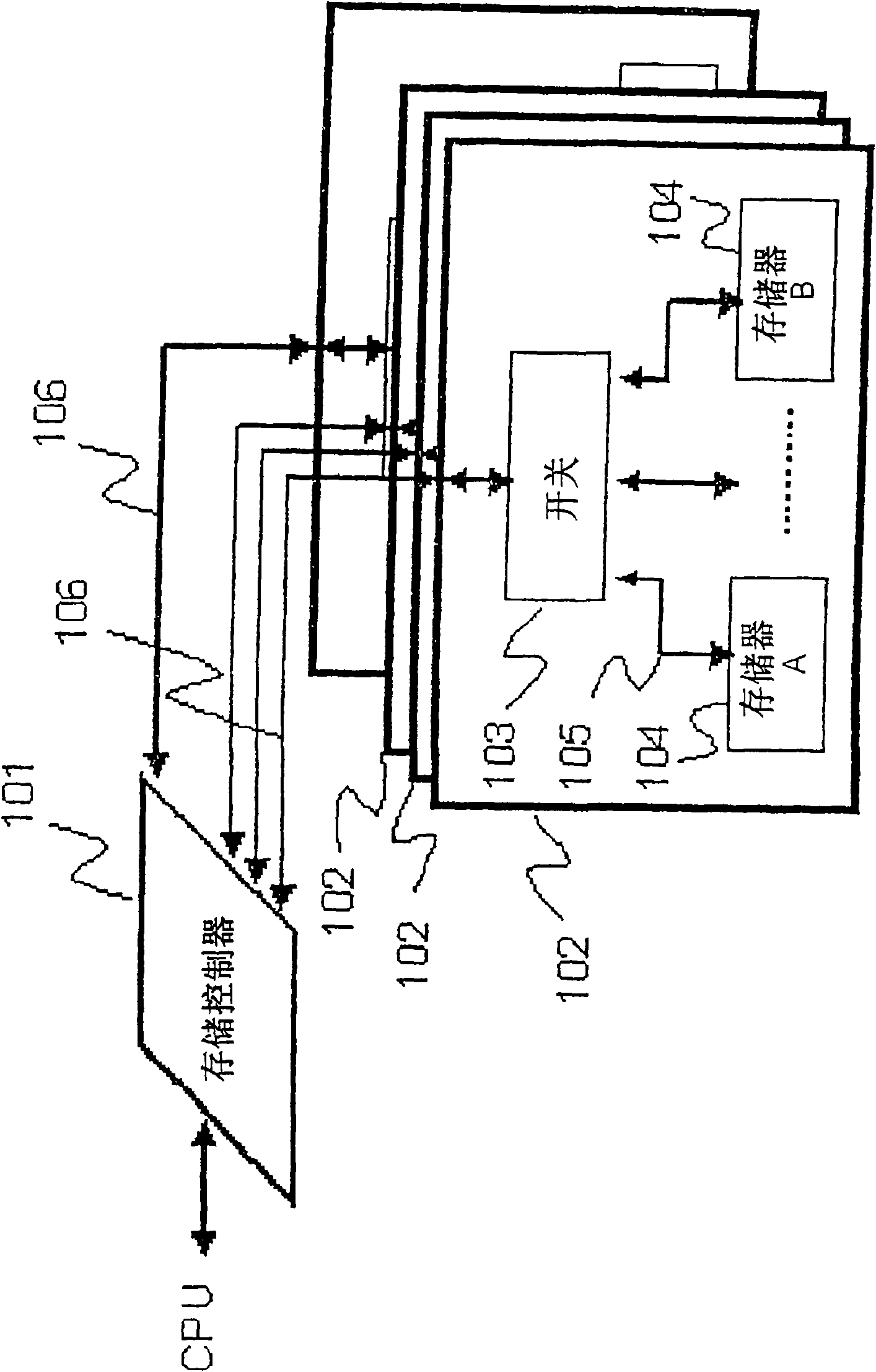
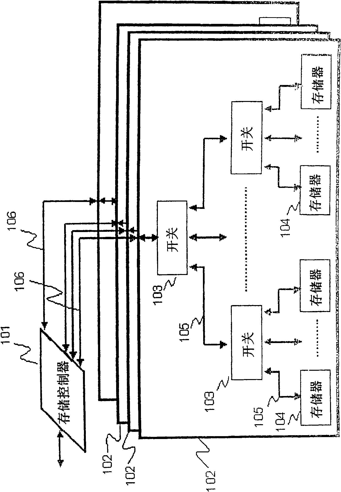
[0051] The present invention will be described below with reference to the accompanying drawings. see figure 1 , the storage system according to the embodiment of the present invention includes: a storage controller 101; a plurality of storages 104, wherein a plurality of storages 104 are connected to a specific position, that is, one end of a corresponding bus 106 through a switch 103 and respective interconnection lines 105, the bus 106 is connected to the storage controller 101.

[0052] Operation of multiple memories 104 including memory A and memory B is controlled by switch 103 . A plurality of memories 104 are formed as respective memory chips 104 , however, switches 103 are formed on individual switch chips 103 . These chips are mounted on the same memory module 102 . In this embodiment, a plurality of storage modules 102 are connected to the storage controller 101 through their respective buses, and a large number of memories are connected to the bus 106 .

[005...


PUM


Abstract

A memory system has a memory controller and a plurality of memories. The plurality of memories are connected via a switch to an end of a bus, which is connected to the memory controller, wherein the plurality of memories are controlled by the switch. By suppressing reflection and loads on the bus, a higher data transmission speed can be obtained.

Description

[0001] This application is a PCT international application with the international filing date of June 20, 2001 and the international application number PCT / JP01 / 05270, which has entered the Chinese national phase, and the national application number is 01811401.6, entitled "High-speed storage system" Divisional application of the application. technical field [0002] The present invention relates to a high-speed storage system, and more particularly, to a storage system with higher transmission speed and higher operating speed, and to a storage interface and a storage chip for such a storage system. Background technique [0003] Figure 18 A traditional storage system is shown. In this figure, a bus 1802 connected to a storage controller 1801 extends in one direction, and is installed in a plurality of ( Figure 18 A plurality of storage modules 1804 on the storage chip 1803 are connected to the bus 1802 in parallel with each other. In this paper, such a bus-connected struc...

Claims


Application Information

Patent Timeline
Patent Type & Authority Applications(China)
IPC IPC(8): G06F3/00G06F12/00G11C11/401G06F13/16G11C7/10
CPCG11C7/1066G11C7/106G06F13/1684G11C7/1006G11C7/10G11C7/1057G11C7/1084G11C7/1087G11C7/1078G11C7/1051G11C7/00
Inventor 深石宗生本村真人相本代志治山品正胜
Owner NEC CORP
Why Eureka
Try Eureka