

Novel wafer fixing structure
A technology for fixing structures and wafers, which is applied in the direction of electric solid-state devices, semiconductor/solid-state device components, electrical components, etc., and can solve problems such as unsatisfactory, different light-emitting angles, and different light-emitting angles.
- Summary
- Abstract
- Description
- Claims
- Application Information
AI Technical Summary
Problems solved by technology
Method used
Image

Examples
Embodiment Construction
[0017] In order to make the technical means, creative features, goals and effects achieved by the present invention easy to understand, the present invention will be further described below in conjunction with specific illustrations.
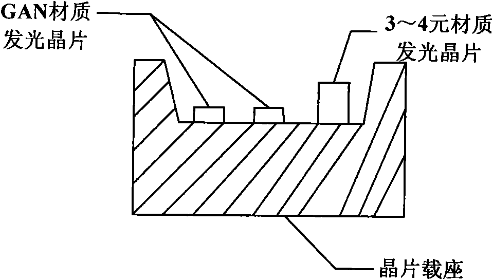
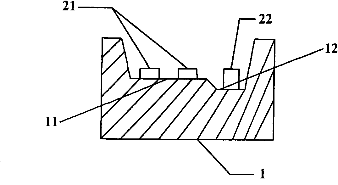
[0018] Such as figure 2 As shown, a novel wafer fixing structure includes a wafer carrier 1 and a light-emitting chip. The wafer carrier 1 is provided with a plane die-bonding area 11, and a recessed die-bonding area 11 is provided in the plane die-bonding area 11 of the wafer carrier 1. The region 12, the planar crystal-bonding region 11 and the recessed crystal-bonding region 12 are respectively used to fix light-emitting chips with different thicknesses.
[0019] In this embodiment, the light-emitting chip includes a GAN material light-emitting chip 21 and a traditional 3-4 element material light-emitting chip 22; since the thickness of the traditional 3-4 element material light-emitting chip 22 is greater than the thickness of the GAN mater...
PUM
 Abstract
Description
Claims
Application Information