Liquid crystal display device mother board

A technology for liquid crystal display devices and mother substrates, applied in nonlinear optics, instruments, optics, etc., capable of solving problems such as detection function failure, short circuit between first metal line 11 and second metal line 12, array substrate test failure, etc. To achieve the effect of reducing short circuit, improving reliability and preventing electrostatic damage

Active Publication Date: 2009-10-28
KUSN INFOVISION OPTOELECTRONICS
View PDF0 Cites 13 Cited by
  • Summary
  • Abstract
  • Description
  • Claims
  • Application Information

AI Technical Summary

Problems solved by technology

[0007] When breakdown occurs at the first overlapping region 13 due to static electricity accumulation, the first metal line 11 and the second metal line 12 used for detection will not be able to realize the function of detecting the array substrate
[0008] It can be seen that in the manufacturing process of the mother substrate of the existing liquid crystal display device, because there is no structure with an electrostatic protection function, it is easy to cause a short circuit between the first metal wire 11 and the second metal wire 12, and the first metal wire 11 and the second metal wire 12 are short-circuited. The function of line 12 used for detection is invalid, which will easily lead to the failure of the test of the array substrate and affect the product yield

Method used


Image

  • Liquid crystal display device mother board
  • Liquid crystal display device mother board
  • Liquid crystal display device mother board

Examples


Embodiment Construction

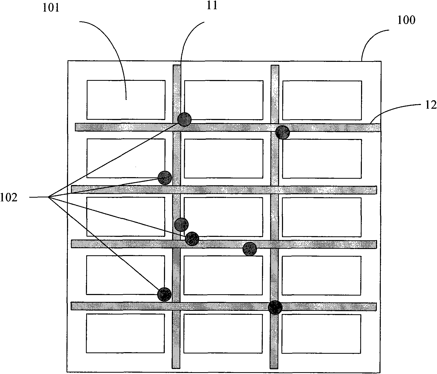
[0022] The object of the present invention is to provide a mother substrate of a liquid crystal display device capable of effectively transferring the position of a metal line used for testing where the static electricity breaks down without affecting the display area of ​​the array substrate.

[0023] In order to make the object, technical solution and advantages of the present invention clearer, the present invention will be further described in detail below with reference to the accompanying drawings and according to specific embodiments.

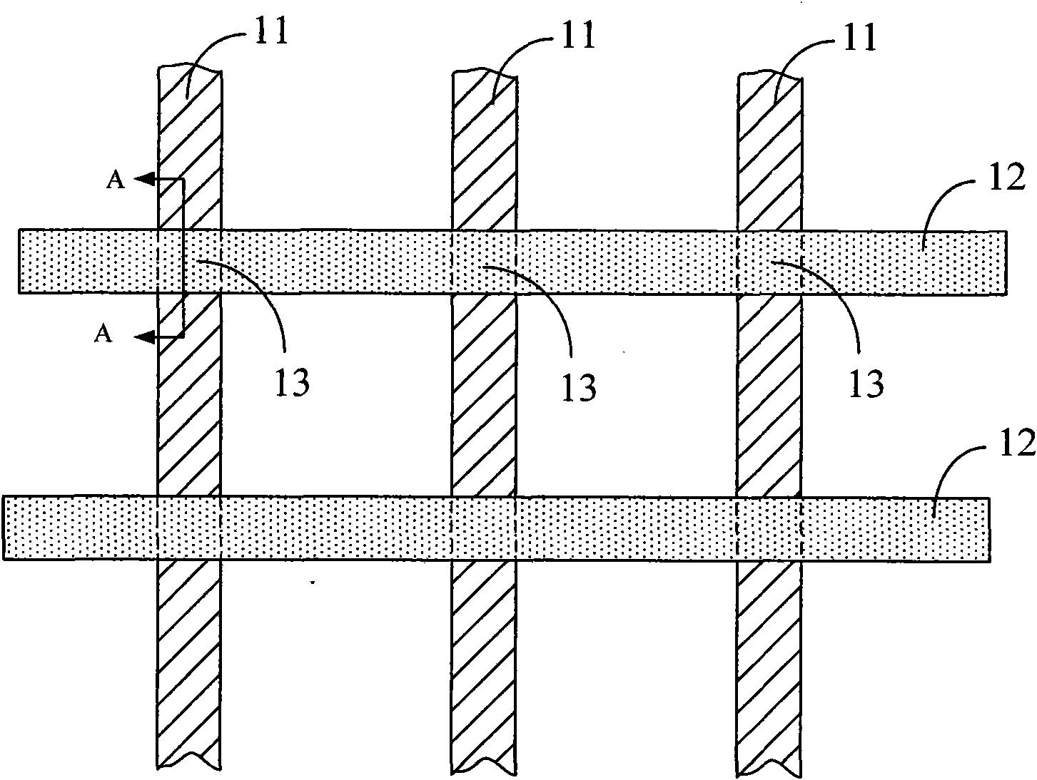
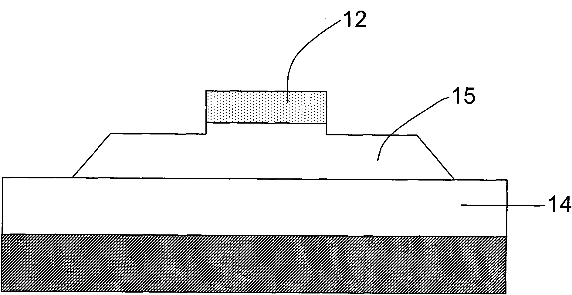
[0024] Figure 4 It is a schematic diagram of the overlapping structure of the local detection metal lines of the mother substrate of the liquid crystal display device of the present invention. Such as Figure 4 As shown, the mother substrate of the liquid crystal display device of the present invention includes a first metal line 41 and a second metal line 42 arranged crosswise for array substrate detection, located in the first overla...


PUM


Abstract

The invention provides a liquid crystal display device mother board, which includes a first metal wire and a second metal wire which are across arranged; and also includes a first overlapping region arranged between the first metal wire and the second metal wire, and a first insulation layer for insulating the first metal wire and the second metal wire; the first metal wire is provided with a first bulge which laterally projects, and the second metal wire is provided with a second bulge which laterally projects; free ends of the first bulge and the second bulge are overlapped mutually, and a second overlapping region between the first bulge and the second bulge is provided with a second insulation layer and a semiconductor layer. By arranging the bulges which laterally project at two sides of the two metal wires and the semiconductor layer with electrostatic charge induction characteristic in the second overlapping region of the two bulges, the liquid crystal display device mother board makes the electrostatic charge accumulated on the mother glass board transfer to the second overlapping region of the bulges of the two metal wires, thereby effectively reducing the phenomenon of short circuit of the two metal wires generated in the first overlapping region.

Description

technical field [0001] The invention relates to the field of liquid crystal displays, in particular to a mother substrate of a liquid crystal display device with an electrostatic protection function. Background technique [0002] Liquid crystal display (LCD) has gradually replaced the monopoly position of cathode ray tube (CRT) displays due to its advantages of high resolution, no flicker, small size and light weight, and has been widely used in mobile phones, notebook computers, personal digital assistants, etc. Shows the field of application. [0003] As liquid crystal displays are widely used, the requirements for display quality are gradually increased, and it is required that the liquid crystal display has as few or no point defects as possible due to bad pixels. A liquid crystal display mainly includes an array substrate, an opposite substrate, and a liquid crystal layer sandwiched between the array substrate and the opposite substrate. The array substrate is usually...

Claims


Application Information

Patent Timeline
Patent Type & Authority Applications(China)
IPC IPC(8): G02F1/136G02F1/13
Inventor 闫秀梅程一凡
Owner KUSN INFOVISION OPTOELECTRONICS
Why Eureka
Try Eureka