Semiconductor device and manufacturing method thereof

A manufacturing method, semiconductor technology, applied in the direction of semiconductor/solid-state device manufacturing, semiconductor devices, semiconductor/solid-state device components, etc., can solve the problem of increasing the amount of particles

Inactive Publication Date: 2009-11-04
SEIKO EPSON CORP
View PDF1 Cites 2 Cited by
  • Summary
  • Abstract
  • Description
  • Claims
  • Application Information

AI Technical Summary

Problems solved by technology

However, if the depth is increased, there is a concern that the amount of particles generated after the laser is irradiated by the laser marking device will increase

Method used


Image

  • Semiconductor device and manufacturing method thereof
  • Semiconductor device and manufacturing method thereof
  • Semiconductor device and manufacturing method thereof

Examples


Embodiment Construction

[0027] Hereinafter, embodiments of the present invention will be described with reference to the drawings.

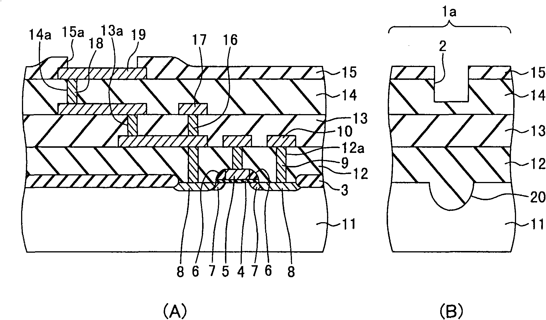
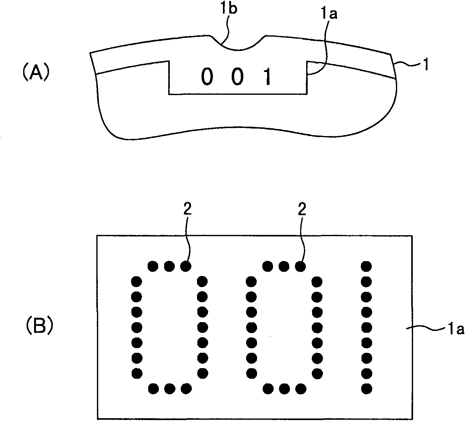
[0028] figure 1 (A), figure 1 (B) is a cross-sectional view for explaining a method of manufacturing a semiconductor device according to an embodiment of the present invention, figure 1 (A) is a cross-sectional view showing a part of a product chip region of a silicon wafer, figure 1 (B) means located in such as figure 1 (A) A cross-sectional view of a part of the print-only area near the notch of the silicon wafer shown. figure 2 (A) means if figure 1 The overall top view of the print-only area shown in (B), figure 2 (B) is for figure 2 (A) shows a magnified top view of the printed wafer ID.

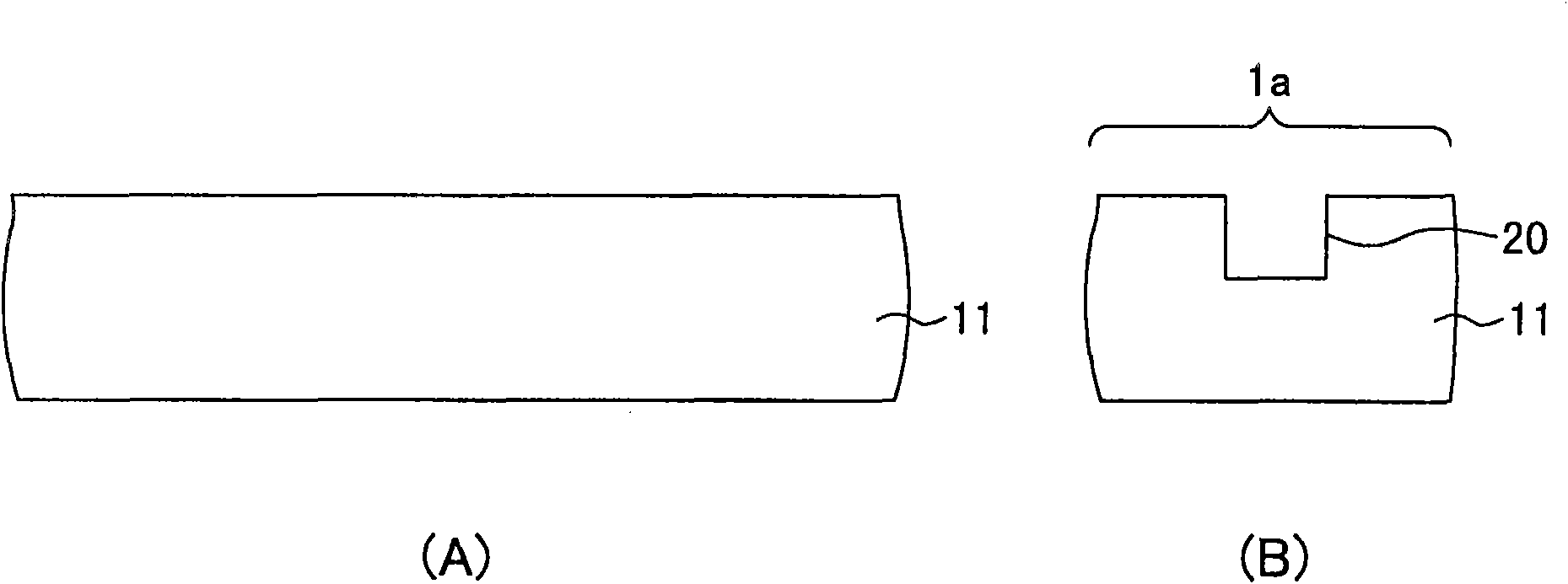
[0029] First, if figure 1 (B) and figure 2 As shown in (A), the wafer ID is printed by a laser marking device on the printing-only area 1a located near the notch 1b of the silicon wafer (silicon substrate) 11 . Thus, a plurality of continuous depressions 20 c...


PUM


Abstract

The present invention provides a semiconductor device capable of using a wafer ID with high vision identity even though in a rear step, and a method for manufacturing the same. The method of the invention for manufacturing the semiconductor device includes steps: printing a first wafer ID (20) on a silicon substrate (11) by a laser identification device; forming a first, a second and a third layer insulation films (12, 13, 14) on the silicon substrate; forming a passivating film (15) on the first, the second and the third layer insulation films (12, 13, 14); and printing a second wafer ID (2) on the passivating film (15) by the laser identification device in a mode of overlapping the first wafer ID (20).

Description

technical field [0001] The present invention relates to a semiconductor device and its manufacturing method, and more particularly to a semiconductor device and its manufacturing method in which a highly visible wafer ID can be used even in a later step. Background technique [0002] image 3 (A), image 3 (B) and Figure 4 (A), Figure 4 (B) is a cross-sectional view for explaining a conventional method of manufacturing a semiconductor device. image 3 (A) and Figure 4 (A) are cross-sectional views showing a part of a product chip (chip) region of a silicon wafer, respectively, image 3 (B) and Figure 4 (B) are respectively located in such as Figure 4 (A) A cross-sectional view of a part of the print-only area near the notch of the silicon wafer shown. [0003] First, if image 3 As shown in (B), the wafer ID is printed on the printing-dedicated area 1a near the notch of the silicon wafer (silicon substrate) 11 by a laser marker. Thus, a plurality of continuous depr...

Claims


Application Information

Patent Timeline
Patent Type & Authority Applications(China)
IPC IPC(8): H01L21/02H01L21/31H01L23/544
Inventor 林正浩椎野刚
Owner SEIKO EPSON CORP
Why Eureka
Try Eureka