Method for monitoring thickness of metal plating layer on surface of plated part

A technology of surface metal and coating thickness, applied in measuring devices, instruments, scientific instruments, etc., can solve the problems of long test time, complex test process, high requirements for electron microscope performance, etc., and achieve the effect of accurate and reliable monitoring results

Inactive Publication Date: 2009-11-11
江门市旭晨科技有限公司
View PDF0 Cites 20 Cited by
  • Summary
  • Abstract
  • Description
  • Claims
  • Application Information

AI Technical Summary

Benefits of technology

This technology uses an SEM - X- ray device that measures how well coatings are being applied onto small areas or large surfaces. It provides quantification capabilities for studying these materials without damaging them during testing.

Problems solved by technology

Technologies used by manufacturers involved in producing electronic components involve controlling their thickness during production processes or inspecting any defects that may occur due to improper deposition techniques like immersion tinning or sprayed paint overcoats. Current solutions have drawbacks including slow response times and complex procedures involving multiple steps. There needs a more efficient way to monitor these thin films without damaging themselves while maintaining good quality standards.

Method used


Image

  • Method for monitoring thickness of metal plating layer on surface of plated part
  • Method for monitoring thickness of metal plating layer on surface of plated part
  • Method for monitoring thickness of metal plating layer on surface of plated part

Examples


Embodiment 1

[0035] This embodiment is used to illustrate the method of the present invention for monitoring the coating thickness on the surface of a plated piece.

[0036] Instrument: JSM-5610LV scanning electron microscope (SEM) produced by Japan JEOL Company

[0037] QUEST energy spectrometer (EDS) produced by American NORAN company

[0038]Test Conditions:

[0039] Scanning electron microscope: accelerating voltage 14KV, beam spot 35nm, load current 70μA, working distance 9mm, magnification 10000 times, select scan3 to scan.

[0040] QUEST energy spectrometer: live time is less than 100 seconds, dead time is more than 25 seconds, ZAF correction, data collection time is 56 seconds, pixel points are 128×128, and the collection time of each pixel point is 0.03 seconds.

[0041] Instrument data processing software: SpectraPlus

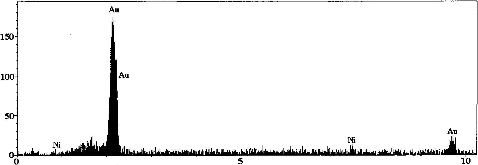
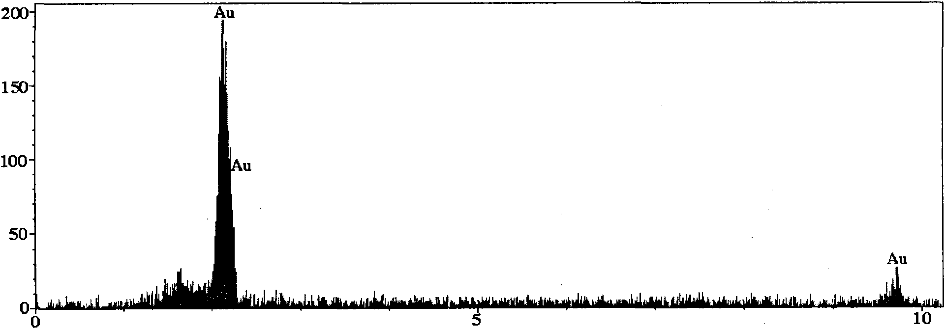
[0042] The base material of the plated part is Cu, and Ni and Au are plated on the base material in turn, the thickness of the Ni layer is 4 μ m, and the Au is...

Embodiment 2

[0045] This embodiment is used to illustrate the method of the present invention for monitoring the coating thickness on the surface of a plated piece.

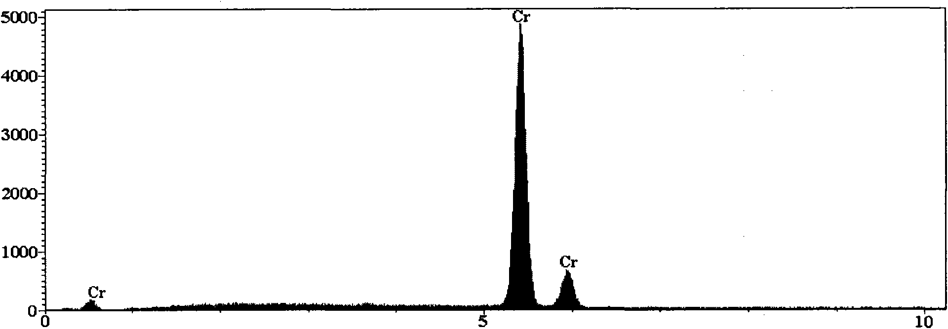
[0046] According to the same method as in Example 1, the difference is that the substrate is plated with Cr and Al in sequence, the thickness of the Cr layer is 5 μm, and the Al is located on the surface, and the accelerating voltage is 20KV. The test results are: 0.3 μm, 0.38 The characteristic peaks of Cr and Al appear in the spectra of standard samples of μm, 0.43 μm, 0.48 μm, 0.5 μm, 0.53 μm, 0.56 μm, 0.6 μm, 0.63 μm and 0.7 μm, among which, the EDS spectrum of the 0.7 μm standard sample Such as image 3 shown. Only the characteristic peaks of Al appear in the spectra of 0.73 μm and 0.8 μm standard samples, among which, the EDS spectra of 0.73 μm standard samples are as follows Figure 4 shown. Such test results indicate that the currently set accelerating voltage can be used to monitor whether the thickness of the sur...

Embodiment 3

[0048] This embodiment is used to illustrate the method of the present invention for monitoring the coating thickness on the surface of a plated piece.

[0049] Instrument: JSM-5610LV scanning electron microscope (SEM) produced by Japan JEOL Company

[0050] QUEST energy spectrometer (EDS) produced by American NORAN company

[0051] Fixed test conditions:

[0052] Scanning electron microscope: working distance 9mm, beam spot 35nm, load current 70μA, magnification 10000 times, select scan3 to scan.

[0053] QUEST energy spectrometer: live time is less than 100 seconds, dead time is more than 25 seconds, ZAF correction, data collection time is 70 seconds, pixel points are 128×128, and the collection time of each pixel point is 0.03 seconds.

[0054] Test conditions that need to be adjusted: Accelerating voltage

[0055] Instrument data processing software: SpectraPlus

[0056] The plated parts are copper-clad laminates (referred to as copper-clad laminates), and the thicknes...


PUM

PropertyMeasurementUnit
Thicknessaaaaaaaaaa
Thicknessaaaaaaaaaa
Thicknessaaaaaaaaaa

Abstract

The invention relates to a method for monitoring the thickness of a metal plating layer on the surface of a plated part. The method comprises the following steps: collecting energy spectrum diagram on the surface of the plated part by adopting an X-ray energy spectrometer and monitoring the thickness of the metal plating layer on the surface of the plated part according to the condition whether the energy spectrum diagram has an incident beam or a characteristic peak of elements which are not contained in the metal plating layer on the surface. Due to the adoption of a method for scanning an electron microscope, i.e. the X-ray energy spectrometer, the thickness of the plating layer on the surface of a minuscular area and a millimeter-level plated part can be monitored. With the qualitative test function, the energy spectrometer can also monitor an alloy plating layer and qualitatively analyze elements on the plating layer, thereby analyzing substances on the plating layer of a blind sample. The method can be used for monitoring the thickness of the plating layer without damaging the sample and ensures an accurate and reliable monitoring result.

Description


Claims


Application Information

Patent Timeline
Owner 江门市旭晨科技有限公司
Why Eureka
Try Eureka