Surface wave device encapsulation structure
A surface wave device and packaging structure technology, applied in the direction of electrical components, impedance networks, etc., can solve problems such as confusion, low qualified rate of finished products, and long process, and achieve the goal of increasing the rate of qualified products, shortening the production process, and ensuring reliability. Effect
- Summary
- Abstract
- Description
- Claims
- Application Information
AI Technical Summary
Problems solved by technology
Method used
Image

Examples
Embodiment 1
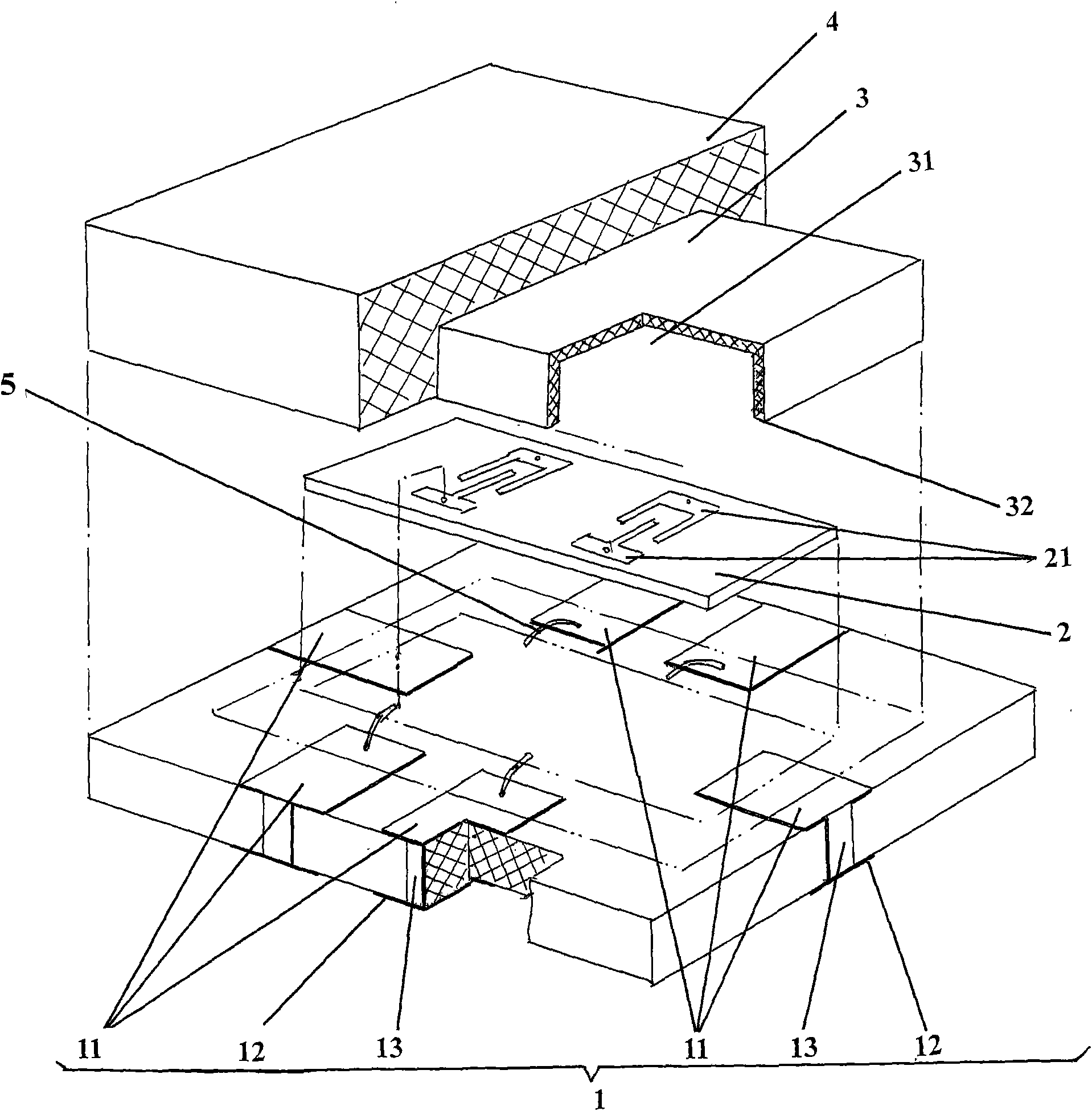
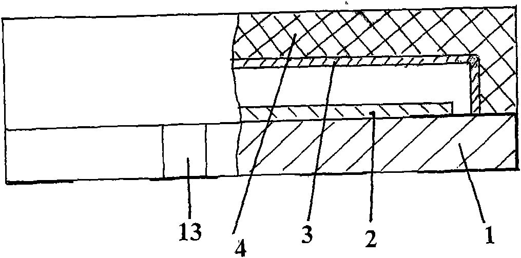
[0020] please see figure 1 with figure 2 , the material with a thickness of 0.5mm is an epoxy resin layer, and copper is coated on both sides of the epoxy resin layer, and the copper clad layer on the surface of one side, that is, the side that is facing upward in the current position shown in the figure, is etched out by an etching process. A set of first electrodes 11 is formed, and a set of second electrodes 12 are etched on the copper clad layer on the other side surface, that is, the side surface facing downward, so as to constitute the printed circuit board 1 shown in the figure. In addition, the first and second electrodes 11 and 12 can also be referred to as front and back electrodes. The surfaces of the first and second electrodes 11 and 12 are all plated with gold. Metallized holes 13 with walls plated with gold implement electrical connections. As a specific implementation, the number of a group of first and second electrodes 11, 12 is obviously not affected by ...
Embodiment 2
[0023] Only the material of the printed circuit board 1 is changed to polytetrafluoroethylene double-sided printed circuit board, and the rest are the same as the description of the first embodiment.
PUM
 Abstract
Description
Claims
Application Information
 - R&D Engineer
- R&D Manager
- IP Professional
- Industry Leading Data Capabilities
- Powerful AI technology
- Patent DNA Extraction
Browse by: Latest US Patents, China's latest patents, Technical Efficacy Thesaurus, Application Domain, Technology Topic.
© 2024 PatSnap. All rights reserved.Legal|Privacy policy|Modern Slavery Act Transparency Statement|Sitemap