Data storage device and data storage method

A data storage and data technology, applied in the direction of memory address/allocation/relocation, etc., can solve the problems affecting the efficiency of memory usage, save storage space and improve the efficiency of system operation.

Active Publication Date: 2010-01-13
VIA TECH INC
View PDF0 Cites 2 Cited by
  • Summary
  • Abstract
  • Description
  • Claims
  • Application Information

AI Technical Summary

Problems solved by technology

Poor logical-physical address mapping will se

Method used


Image

  • Data storage device and data storage method
  • Data storage device and data storage method
  • Data storage device and data storage method

Examples


Embodiment Construction

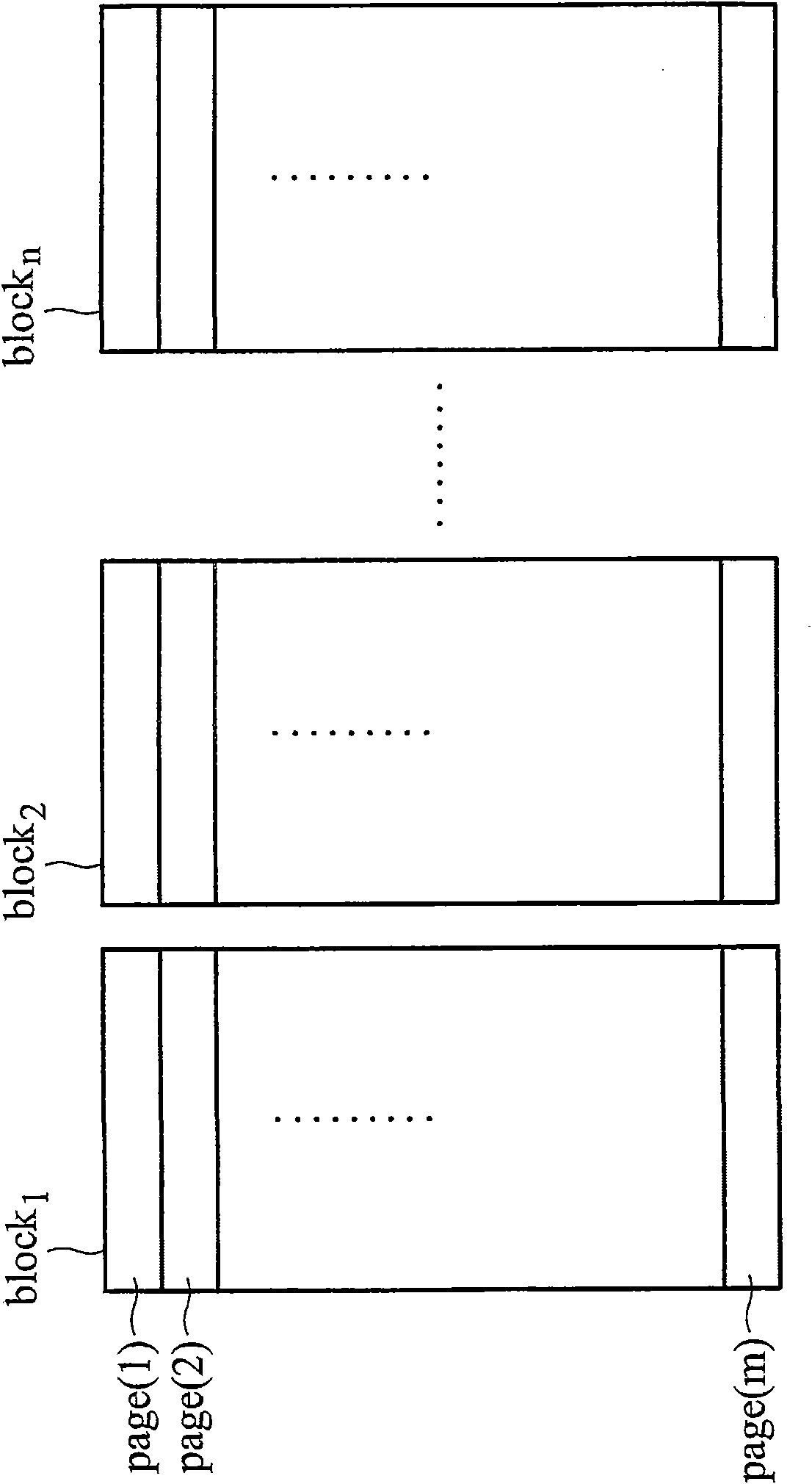
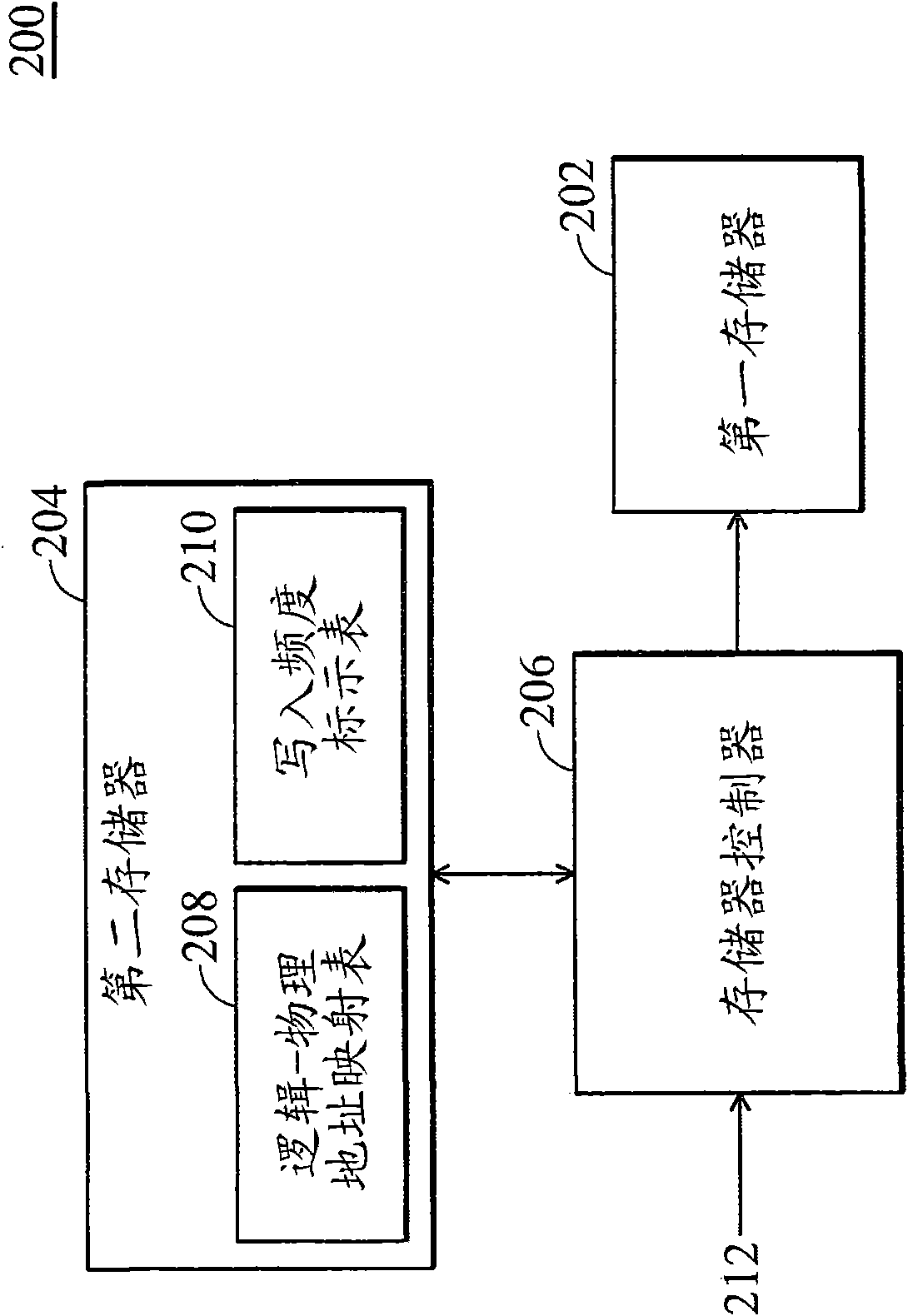
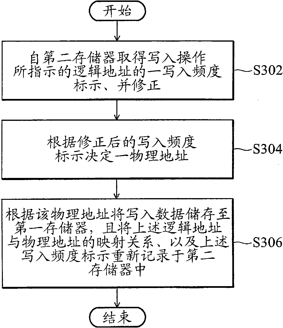
[0018] figure 2 An embodiment of the data storage device of the present invention is illustrated in a block diagram, wherein a write operation is particularly illustrated. The data storage device 200 includes a first memory 202 , a second memory 204 and a memory controller 206 . The first memory 202 is an element that actually stores data, and its space is divided by physical addresses. The address information included in the write operation command and the read operation command received by the data storage device 200 is called a logical address. The mapping relationship between the logical address and the physical address is recorded in the second memory 204 as a logical-physical address mapping table 208 . In addition, the present invention also utilizes the space of the second memory 204 to provide a write frequency mark for each logical address to indicate the frequency with which the logical address is written, and the corresponding relationship between the logical ad...


PUM


Abstract

The invention provides a data storage device and a data storage method. The data storage device comprises a first memory and a memory controller, wherein the first memory is a component for practically storing data, and space of the first memory is divided by a physical address; the address information viewed in a logical operation stage is called a logical address; and the memory controller receives the logical address and writing data under the writing operation, corrects a writing frequency mark of the logical address and decides the corresponding physical address of the logical address on the first memory according to the corrected writing frequency mark so as to write the writing data into the physical address of the first memory. The invention greatly improves the operating efficiency of a system, particularly the efficiency during block release and expresses the written frequency of the logical address by fewer storage spaces, thereby greatly saving the storing space.

Description

technical field [0001] The invention relates to a data storage device and a used data storage method. Background technique [0002] In addition to hard disks, optical disks, etc., memory is often used to store data. Taking NAND flash memory (NAND Flash) as an example, it is often used as a storage unit in portable electronic devices. For example, common mp3 players on the market often use NAND flash memory to store data. [0003] figure 1 Diagram illustrating the physical space of NAND flash memory. A NAND flash memory has multiple blocks (blocks, numbered as block 1 、block 2 ,..., block n ), and the blocks each include a plurality of pages (pages, for example, the block block1 includes a plurality of pages page(1), page(2), . . . , page(m)). The writing operation of NAND flash memory is usually in the unit of “page”, and one page is written into the memory page by page; when the storage space is exhausted, the memory space is usually released in the unit of “block”. ...

Claims


Application Information

Patent Timeline
IPC IPC(8): G06F12/02G06F12/06
Inventor 张博
Owner VIA TECH INC
Why Eureka
Try Eureka